- 您现在的位置:买卖IC网 > PDF目录10654 > AD9484BCPZ-500 (Analog Devices Inc)IC ADC 8BIT 500MSPS 56LFCSP PDF资料下载
参数资料
| 型号: | AD9484BCPZ-500 |
| 厂商: | Analog Devices Inc |
| 文件页数: | 6/24页 |
| 文件大小: | 0K |
| 描述: | IC ADC 8BIT 500MSPS 56LFCSP |
| 标准包装: | 1 |
| 位数: | 8 |
| 采样率(每秒): | 500M |
| 数据接口: | 串行,SPI? |
| 转换器数目: | 1 |
| 功率耗散(最大): | 720mW |
| 电压电源: | 模拟和数字 |
| 工作温度: | -40°C ~ 85°C |
| 安装类型: | 表面贴装 |
| 封装/外壳: | 56-VFQFN 裸露焊盘,CSP |
| 供应商设备封装: | 56-LFCSP-VQ(8x8) |
| 包装: | 托盘 |
| 输入数目和类型: | 1 个差分,双极 |
AD9484
Rev. A | Page 14 of 24
THEORY OF OPERATION
The AD9484 architecture consists of a front-end sample-and-
hold amplifier (SHA) followed by a pipelined switched capacitor
ADC. The quantized outputs from each stage are combined into
a final 8-bit result in the digital correction logic. The pipelined
architecture permits the first stage to operate on a new input
sample, whereas the remaining stages operate on preceding
samples. Sampling occurs on the rising edge of the clock.
Each stage of the pipeline, excluding the last, consists of a low
resolution flash ADC connected to a switched capacitor DAC
and interstage residue amplifier (MDAC). The residue amplifier
magnifies the difference between the reconstructed DAC output
and the flash input for the next stage in the pipeline. One bit of
redundancy is used in each stage to facilitate digital correction
of flash errors. The last stage simply consists of a flash ADC.
The input stage contains a differential SHA that can be ac- or
dc-coupled in differential or single-ended mode. The output
staging block aligns the data, carries out the error correction,
and passes the data to the output buffers. The output buffers
are powered from a separate supply, allowing adjustment of the
output voltage swing. During power-down, the output buffers
enter a high impedance state.
ANALOG INPUT AND VOLTAGE REFERENCE
The analog input to the AD9484 is a differential buffer. For best
dynamic performance, match the source impedances driving
VIN+ and VIN such that common-mode settling errors are
symmetrical. The analog input is optimized to provide superior
wideband performance and requires that the analog inputs be
driven differentially. SNR and SINAD performance degrades
significantly if the analog input is driven with a single-ended
signal.
A wideband transformer, such as Mini-Circuits ADT1-1WT,
can provide the differential analog inputs for applications that
require a single-ended-to-differential conversion. Both analog
inputs are self-biased by an on-chip reference to a nominal 1.7 V.
An internal differential voltage reference creates positive and
negative reference voltages that define the 1.5 V p-p fixed span
of the ADC core. This internal voltage reference can be adjusted
by means of SPI control. See the AD9484 Configuration Using
the SPI section for more details.
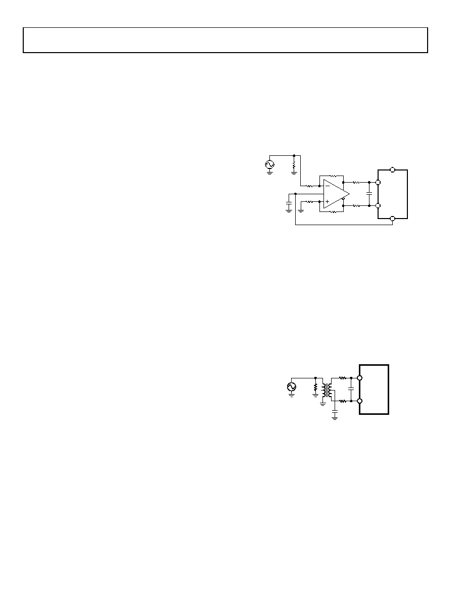
Differential Input Configurations
Optimum performance is achieved while driving the AD9484
in a differential input configuration. For baseband applications,
the AD8138 differential driver provides excellent performance
and a flexible interface to the ADC. The output common-mode
voltage of the AD8138 is easily set to AVDD/2 + 0.5 V, and the
driver can be configured in a Sallen-Key filter topology to pro-
vide band limiting of the input signal.
VIN+
VIN–
AVDD
CML
AD8138
523
499
33
49.9
1V p-p
0.1F
20pF
AD9484
0
961
5-
0
13
Figure 28. Differential Input Configuration Using the AD8138
At input frequencies in the second Nyquist zone and above, the
performance of most amplifiers may not be adequate to achieve
the true performance of the AD9484. This is especially true in
IF undersampling applications where frequencies in the 70 MHz
to 100 MHz range are being sampled. For these applications,
differential transformer coupling is the recommended input
configuration. The signal characteristics must be considered
when selecting a transformer. Most RF transformers saturate at
frequencies below a few megahertz (MHz), and excessive signal
power can cause core saturation, which leads to distortion.
In any configuration, the value of the shunt capacitor, C (see
Figure 30), is dependent on the input frequency and may need
to be reduced or removed.
VIN+
VIN–
15
50
1.5V p-p
0.1F
2pF
AD9484
096
15-
0
14
Figure 29. Differential Transformer—Coupled Configuration
As an alternative to using a transformer-coupled input at frequen-
cies in the second Nyquist zone, the AD8352 differential driver
can be used (see Figure 30).
相关PDF资料 |
PDF描述 |
|---|---|
| MAX996ESD+T | IC COMPARATOR R-R 14-SOIC |
| VI-21M-IW-F1 | CONVERTER MOD DC/DC 10V 100W |
| VE-B1K-MX-F3 | CONVERTER MOD DC/DC 40V 75W |
| LTC2252IUH#PBF | IC ADC 12-BIT 105MSPS 3V 32-QFN |
| MAX995EUD+T | IC COMPARATOR R-R 14-TSSOP |
相关代理商/技术参数 |
参数描述 |
|---|---|
| AD9484BCPZRL7-500 | 功能描述:IC ADC 8BIT 500MSPS 56LFCSP RoHS:是 类别:集成电路 (IC) >> 数据采集 - 模数转换器 系列:- 标准包装:1 系列:- 位数:14 采样率(每秒):83k 数据接口:串行,并联 转换器数目:1 功率耗散(最大):95mW 电压电源:双 ± 工作温度:0°C ~ 70°C 安装类型:通孔 封装/外壳:28-DIP(0.600",15.24mm) 供应商设备封装:28-PDIP 包装:管件 输入数目和类型:1 个单端,双极 |
| AD9500 | 制造商:AD 制造商全称:Analog Devices 功能描述:Digitally Programmable Delay Generator |
| AD9500BP | 制造商:Rochester Electronics LLC 功能描述: 制造商:Analog Devices 功能描述: |
| AD9500BP-REEL | 制造商:Analog Devices 功能描述:Digitally Programmable Delay Generator 28-Pin PLCC T/R |
| AD9500BQ | 制造商:AD 制造商全称:Analog Devices 功能描述:Digitally Programmable Delay Generator |
发布紧急采购,3分钟左右您将得到回复。