- 您现在的位置:买卖IC网 > PDF目录10654 > AD9484BCPZ-500 (Analog Devices Inc)IC ADC 8BIT 500MSPS 56LFCSP PDF资料下载
参数资料
| 型号: | AD9484BCPZ-500 |
| 厂商: | Analog Devices Inc |
| 文件页数: | 8/24页 |
| 文件大小: | 0K |
| 描述: | IC ADC 8BIT 500MSPS 56LFCSP |
| 标准包装: | 1 |
| 位数: | 8 |
| 采样率(每秒): | 500M |
| 数据接口: | 串行,SPI? |
| 转换器数目: | 1 |
| 功率耗散(最大): | 720mW |
| 电压电源: | 模拟和数字 |
| 工作温度: | -40°C ~ 85°C |
| 安装类型: | 表面贴装 |
| 封装/外壳: | 56-VFQFN 裸露焊盘,CSP |
| 供应商设备封装: | 56-LFCSP-VQ(8x8) |
| 包装: | 托盘 |
| 输入数目和类型: | 1 个差分,双极 |
AD9484
Rev. A | Page 16 of 24
OPTIONAL
100
0.1F
501
150 RESISTOR IS OPTIONAL.
CLK–
CLK+
ADC
AD9484
VCC
1k
CLOCK
INPUT
AD951x
CMOS DRIVER
096
15-
024
Figure 34. Single-Ended 1.8 V CMOS Input Clock (Up to 200 MHz)
Clock Duty Cycle Considerations
Typical high speed ADCs use both clock edges to generate a
variety of internal timing signals. As a result, these ADCs may
be sensitive to clock duty cycle. A 5% tolerance is commonly
required on the clock duty cycle to maintain dynamic performance
characteristics. The AD9484 contains a duty cycle stabilizer (DCS)
that retimes the nonsampling edge, providing an internal clock
signal with a nominal 50% duty cycle. This allows a wide range
of clock input duty cycles without affecting the performance of
the AD9484. When the DCS is on, noise and distortion perfor-
mance are nearly flat for a wide range of duty cycles.
The duty cycle stabilizer uses a delay-locked loop (DLL) to
create the nonsampling edge. As a result, any changes to the
sampling frequency require approximately 15 clock cycles
to allow the DLL to acquire and lock to the new rate.
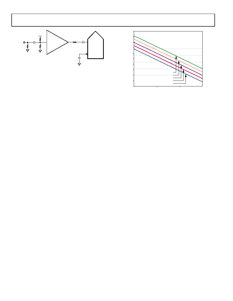
Clock Jitter Considerations
High speed, high resolution ADCs are sensitive to the quality of the
clock input. The degradation in SNR at a given input frequency
(fA) due only to aperture jitter (tJ) can be calculated by
SNR Degradation = 20 × log10(1/2 × π × fA × tJ)
In this equation, the rms aperture jitter represents the root mean
square of all jitter sources, including the clock input, analog input
signal, and ADC aperture jitter specifications. IF undersampling
applications are particularly sensitive to jitter (see Figure 35).
Treat the clock input as an analog signal in cases where aperture
jitter may affect the dynamic range of the AD9484. Separate the
power supplies for clock drivers from the ADC output driver
supplies to avoid modulating the clock signal with digital noise.
Low jitter, crystal-controlled oscillators make the best clock
sources. If the clock is generated from another type of source
(by gating, dividing, or other methods), it should be retimed by
the original clock at the last step.
Application Note for more in-depth information about jitter
performance as it relates to ADCs (visit www.analog.com).
1
10
100
1000
16 BITS
14 BITS
12 BITS
30
40
50
60
70
80
90
100
110
120
130
0.125ps
0.25ps
0.5ps
1.0ps
2.0ps
ANALOG INPUT FREQUENCY (MHz)
10 BITS
8 BITS
RMS CLOCK JITTER REQUIREMENT
S
N
R
(
d
B)
0
9
615
-01
9
Figure 35. Ideal SNR vs. Input Frequency and Jitter
POWER DISSIPATION AND POWER-DOWN MODE
As shown in Figure 18, the power dissipated by the AD9484 is
proportional to its sample rate. The digital power dissipation
does not vary much because it is determined primarily by the
DRVDD supply and bias current of the LVDS output drivers.
By asserting PDWN (Pin 29) high, the AD9484 is placed in
standby mode or full power-down mode, as determined by the
contents of Serial Port Register 08. Reasserting the PDWN pin
low returns the AD9484 to its normal operational mode.
An additional standby mode is supported by means of varying
the clock input. When the clock rate falls below 50 MHz, the
AD9484 assumes a standby state. In this case, the biasing network
and internal reference remain on, but digital circuitry is powered
down. Upon reactivating the clock, the AD9484 resumes normal
operation after allowing for the pipeline latency.
DIGITAL OUTPUTS
Digital Outputs and Timing
The AD9484 differential outputs conform to the ANSI-644
LVDS standard on default power-up. This can be changed to a
low power, reduced signal option similar to the IEEE 1596.3
standard using the SPI. This LVDS standard can further reduce
the overall power dissipation of the device, which reduces the
power by ~39 mW. See the Memory Map section for more infor-
mation. The LVDS driver current is derived on chip and sets
the output current at each output equal to a nominal 3.5 mA.
A 100 Ω differential termination resistor placed at the LVDS
receiver inputs results in a nominal 350 mV swing at the receiver.
The AD9484 LVDS outputs facilitate interfacing with LVDS
receivers in custom ASICs and FPGAs that have LVDS capability
for superior switching performance in noisy environments.
Single point-to-point net topologies are recommended with a
100 Ω termination resistor placed as close to the receiver as
possible. No far-end receiver termination or poor differential
trace routing may result in timing errors. It is recommended
that the trace length be no longer than 24 inches and that the
相关PDF资料 |
PDF描述 |
|---|---|
| MAX996ESD+T | IC COMPARATOR R-R 14-SOIC |
| VI-21M-IW-F1 | CONVERTER MOD DC/DC 10V 100W |
| VE-B1K-MX-F3 | CONVERTER MOD DC/DC 40V 75W |
| LTC2252IUH#PBF | IC ADC 12-BIT 105MSPS 3V 32-QFN |
| MAX995EUD+T | IC COMPARATOR R-R 14-TSSOP |
相关代理商/技术参数 |
参数描述 |
|---|---|
| AD9484BCPZRL7-500 | 功能描述:IC ADC 8BIT 500MSPS 56LFCSP RoHS:是 类别:集成电路 (IC) >> 数据采集 - 模数转换器 系列:- 标准包装:1 系列:- 位数:14 采样率(每秒):83k 数据接口:串行,并联 转换器数目:1 功率耗散(最大):95mW 电压电源:双 ± 工作温度:0°C ~ 70°C 安装类型:通孔 封装/外壳:28-DIP(0.600",15.24mm) 供应商设备封装:28-PDIP 包装:管件 输入数目和类型:1 个单端,双极 |
| AD9500 | 制造商:AD 制造商全称:Analog Devices 功能描述:Digitally Programmable Delay Generator |
| AD9500BP | 制造商:Rochester Electronics LLC 功能描述: 制造商:Analog Devices 功能描述: |
| AD9500BP-REEL | 制造商:Analog Devices 功能描述:Digitally Programmable Delay Generator 28-Pin PLCC T/R |
| AD9500BQ | 制造商:AD 制造商全称:Analog Devices 功能描述:Digitally Programmable Delay Generator |
发布紧急采购,3分钟左右您将得到回复。