- 您现在的位置:买卖IC网 > PDF目录1987 > AD9515BCPZ-REEL7 (Analog Devices Inc)IC CLOCK DIST 2OUT PLL 32LFCSP PDF资料下载
参数资料
| 型号: | AD9515BCPZ-REEL7 |
| 厂商: | Analog Devices Inc |
| 文件页数: | 15/28页 |
| 文件大小: | 0K |
| 描述: | IC CLOCK DIST 2OUT PLL 32LFCSP |
| 设计资源: | Low Jitter Sampling Clock Generator for High Performance ADCs Using AD9958/9858 and AD9515 (CN0109) |
| 标准包装: | 1,500 |
| 类型: | 扇出缓冲器(分配),除法器 |
| PLL: | 无 |
| 输入: | 时钟 |
| 输出: | CMOS,LVDS,LVPECL |
| 电路数: | 1 |
| 比率 - 输入:输出: | 1:2 |
| 差分 - 输入:输出: | 是/是 |
| 频率 - 最大: | 1.6GHz |
| 除法器/乘法器: | 是/无 |
| 电源电压: | 3.135 V ~ 3.465 V |
| 工作温度: | -40°C ~ 85°C |
| 安装类型: | 表面贴装 |
| 封装/外壳: | 32-VFQFN 裸露焊盘,CSP |
| 供应商设备封装: | 32-LFCSP-VQ(5x5) |
| 包装: | 带卷 (TR) |
| 配用: | AD9515/PCBZ-ND - BOARD EVAL CLOCK 2CH AD9515 |
第1页第2页第3页第4页第5页第6页第7页第8页第9页第10页第11页第12页第13页第14页当前第15页第16页第17页第18页第19页第20页第21页第22页第23页第24页第25页第26页第27页第28页
AD9515
Data Sheet
Rev. A | Page 22 of 28
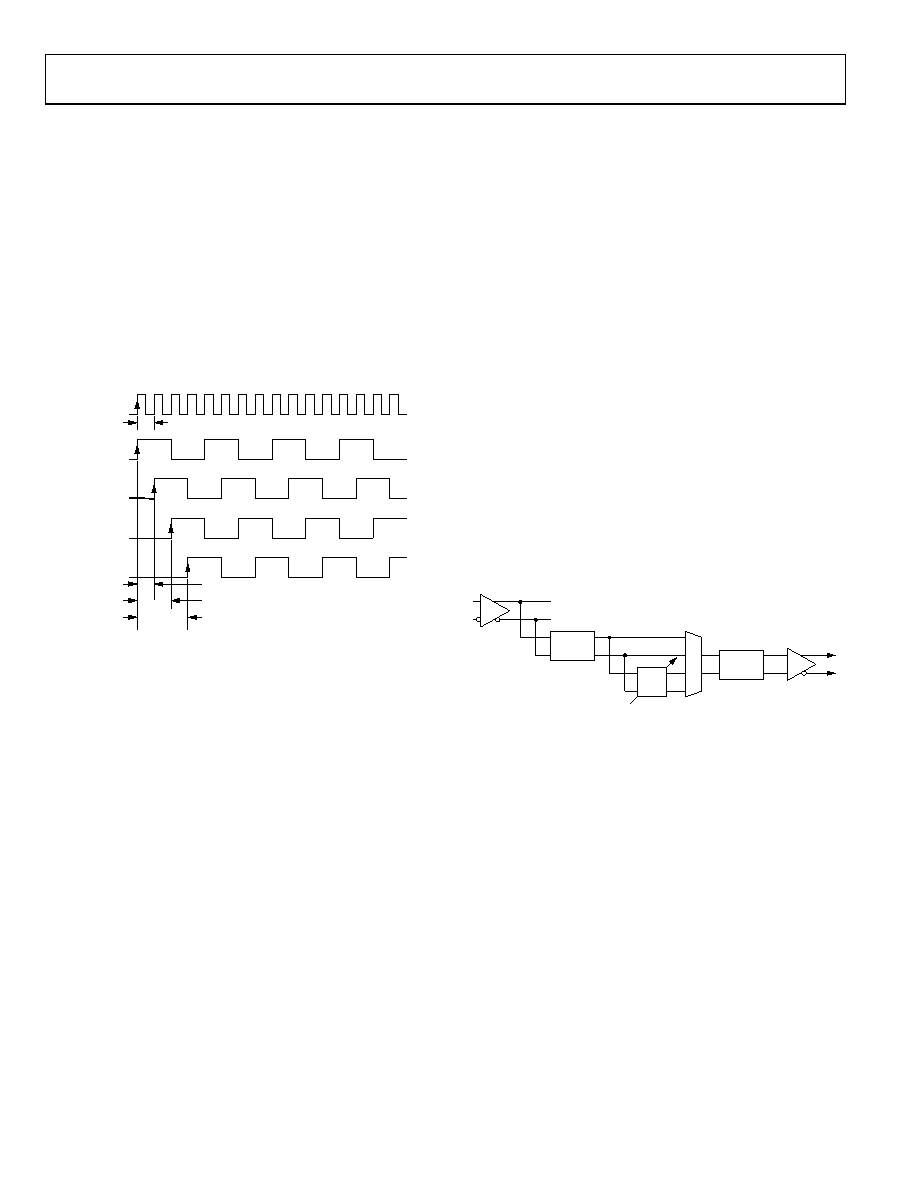
DIVIDER PHASE OFFSET
The phase offset of OUT0 and OUT1 can be selected (see Table 12
to Table 15). This allows the relative phase of OUT0 and OUT1
to be set.
After a SYNC operation (see the Synchronization section), the
phase offset word of each divider determines the number of
input clock (CLK) cycles to wait before initiating a clock output
edge. By giving each divider a different phase offset, output-to-
output delays can be set in increments of the fast clock period, tCLK.
Figure 29 shows four cases, each with the divider set to divide = 4.
By incrementing the phase offset from 0 to 3, the output is
offset from the initial edge by a multiple of tCLK.
0
15
4
1
2
3
5
9
6
7
8
10
14
11
12
13
tCLK
CLOCK INPUT
CLK
DIVIDER OUTPUT
DIV = 4
PHASE = 0
PHASE = 1
PHASE = 2
PHASE = 3
tCLK
2 × tCLK
3 × tCLK
05597-024
Figure 29. Phase Offset—Divider Set for Divide = 4, Phase Set from 0 to 2
For example:
CLK = 491.52 MHz
tCLK = 1/491.52 = 2.0345 ns
For Divide = 4:
Phase Offset 0 = 0 ns
Phase Offset 1 = 2.0345 ns
Phase Offset 2 = 4.069 ns
Phase Offset 3 = 6.104 ns
The outputs can also be described as:
Phase Offset 0 = 0°
Phase Offset 1 = 90°
Phase Offset 2 = 180°
Phase Offset 3 = 270°
Setting the phase offset to Phase = 4 results in the same relative
phase as Phase = 0° or 360°.
The resolution of the phase offset is set by the fast clock period
(tCLK) at CLK. The maximum unique phase offset is less than the
divide ratio, up to a phase offset of 15.
Phase offsets can be related to degrees by calculating the phase
step for a particular divide ratio:
Phase Step = 360°/Divide Ratio
Using some of the same examples:
Divide = 4
Phase Step = 360°/4 = 90°
Unique Phase Offsets in Degrees Are Phase = 0°, 90°,
180°, 270°
Divide = 9
Phase Step = 360°/9 = 40°
Unique Phase Offsets in Degrees Are Phase = 0°, 40°, 80°,
120°, 160°, 200°, 240°, 280°, 320°
DELAY BLOCK
OUT1 includes an analog delay element that gives variable time
delays (ΔT) in the clock signal passing through that output.
÷N
SELECT
LVDS
CMOS
T
MUX
OUTPUT
DRIVER
FINE DELAY ADJUST
(16 STEPS)
FULL SCALE : 1.5ns, 5ns, 10ns
CLOCK INPUT
OUT1 ONLY
05596-025
Figure 30. Analog Delay Block
The amount of delay that can be used is determined by the
output frequency. The amount of delay is limited to less than
one-half cycle of the clock period. For example, for a 10 MHz
clock, the delay can extend to the full 10 ns maximum. However,
for a 100 MHz clock, the maximum delay is less than 5 ns (or
half of the period).
The AD9515 allows for the selection of three full-scale delays,
1.5 ns, 5 ns, and 10 ns, set by delay full scale (see Table 10). Each
of these full-scale delays can be scaled by 16 fine adjustment
values, which are set by the delay word (see Table 14 and Table 15).
The delay block adds some jitter to the output. This means that
the delay function should be used primarily for clocking digital
chips, such as FPGA, ASIC, DUC, and DDC, rather than for
supplying a sample clock for data converters. The jitter is higher
for longer full scales because the delay block uses a ramp and
trip points to create the variable delay. A longer ramp means
more noise has a chance of being introduced.
相关PDF资料 |
PDF描述 |
|---|---|
| AD9516-0BCPZ | IC CLOCK GEN 2.8GHZ VCO 64-LFCSP |
| AD9516-1BCPZ-REEL7 | IC CLOCK GEN 2.5GHZ VCO 64-LFCSP |
| AD9516-2BCPZ | IC CLOCK PLL/VCO 2.2GHZ 64LFCSP |
| AD9516-3BCPZ-REEL7 | IC CLOCK PLL/VCO 2GHZ 64LFCSP |
| AD9516-4BCPZ-REEL7 | IC CLOCK GEN 1.8GHZ VCO 64-LFCSP |
相关代理商/技术参数 |
参数描述 |
|---|---|
| AD95160 | 制造商:AD 制造商全称:Analog Devices 功能描述:14-Channel Clock Generator with Integrated 2.8 GHz VCO |
| AD9516-0 | 制造商:AD 制造商全称:Analog Devices 功能描述:14-Output Clock Generator with Integrated 2.8 GHz VCO |
| AD9516-0/PCBZ | 功能描述:IC CLOCK GEN 2.8GHZ VCO 64-LFCSP RoHS:是 类别:编程器,开发系统 >> 评估演示板和套件 系列:- 标准包装:1 系列:- 主要目的:电信,线路接口单元(LIU) 嵌入式:- 已用 IC / 零件:IDT82V2081 主要属性:T1/J1/E1 LIU 次要属性:- 已供物品:板,电源,线缆,CD 其它名称:82EBV2081 |
| AD9516-0_07 | 制造商:AD 制造商全称:Analog Devices 功能描述:14-Output Clock Generator with Integrated 2.8 GHz VCO |
| AD9516-0BCPZ | 功能描述:IC CLOCK GEN 2.8GHZ VCO 64-LFCSP RoHS:是 类别:集成电路 (IC) >> 时钟/计时 - 时钟发生器,PLL,频率合成器 系列:- 标准包装:2,000 系列:- 类型:PLL 时钟发生器 PLL:带旁路 输入:LVCMOS,LVPECL 输出:LVCMOS 电路数:1 比率 - 输入:输出:2:11 差分 - 输入:输出:是/无 频率 - 最大:240MHz 除法器/乘法器:是/无 电源电压:3.135 V ~ 3.465 V 工作温度:0°C ~ 70°C 安装类型:表面贴装 封装/外壳:32-LQFP 供应商设备封装:32-TQFP(7x7) 包装:带卷 (TR) |
发布紧急采购,3分钟左右您将得到回复。