- 您现在的位置:买卖IC网 > PDF目录16534 > AD9518-0A/PCBZ (Analog Devices Inc)BOARD EVALUATION FOR AD9518-0A PDF资料下载
参数资料
| 型号: | AD9518-0A/PCBZ |
| 厂商: | Analog Devices Inc |
| 文件页数: | 18/64页 |
| 文件大小: | 0K |
| 描述: | BOARD EVALUATION FOR AD9518-0A |
| 设计资源: | AD9518 Eval Brd Schematics AD9518 Gerber Files AD9518-0 BOM |
| 标准包装: | 1 |
| 主要目的: | 计时,时钟发生器 |
| 嵌入式: | 否 |
| 已用 IC / 零件: | AD9518-0A |
| 主要属性: | 2 输入,6 输出,2.8GHz VCO |
| 次要属性: | LVPECL 输出逻辑 |
| 已供物品: | 板 |
第1页第2页第3页第4页第5页第6页第7页第8页第9页第10页第11页第12页第13页第14页第15页第16页第17页当前第18页第19页第20页第21页第22页第23页第24页第25页第26页第27页第28页第29页第30页第31页第32页第33页第34页第35页第36页第37页第38页第39页第40页第41页第42页第43页第44页第45页第46页第47页第48页第49页第50页第51页第52页第53页第54页第55页第56页第57页第58页第59页第60页第61页第62页第63页第64页
Data Sheet
AD9518-0
Rev. C | Page 25 of 64
PROGRAMMABLE
N DELAY
REFIN (REF1)
REFIN (REF2)
CLK
REF1
REF2
AD9518-1
STATUS
R
DIVIDER
VCO STATUS
PROGRAMMABLE
R DELAY
REFERENCE
SWITCHOVER
REF_ SEL
CPRSET VCP
VS
GND
RSET
DISTRIBUTION
REFERENCE
REFMON
CP
STATUS
LD
P, P + 1
PRESCALER
A/B
COUNTERS
N DIVIDER
BYPASS
LF
LOW DROPOUT
REGULATOR (LDO)
VCO
PHASE
FREQUENCY
DETECTOR
LOCK
DETECT
CHARGE
PUMP
PL
L
RE
F
E
RE
N
CE
HOLD
OUT0
OUT1
OUT0
OUT1
LVPECL
DIVIDE BY
1 TO 32
OUT2
OUT3
OUT2
OUT3
LVPECL
DIVIDE BY
1 TO 32
DIVIDE BY
1 TO 32
0
1
PD
SYNC
RESET
SCLK
SDIO
SDO
CS
DIGITAL
LOGIC
SERIAL
CONTROL
PORT
DIVIDE BY
2, 3, 4, 5, OR 6
06
43
0-
02
8
OUT4
OUT5
OUT4
OUT5
LVPECL
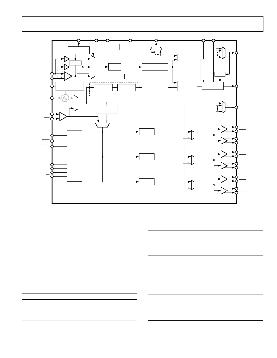
Figure 30. Clock Distribution or External VCO < 1600 MHz
Clock Distribution or External VCO < 1600 MHz
When the external clock source to be distributed or the external
VCO/VCXO is less than 1600 MHz, a configuration that bypasses
the VCO divider can be used. This configuration differs from the
1600 MHz section only in that the VCO divider (divide-by-2/
divide-by-3/divide-by-4/divide-by-5/divide-by-6) is bypassed.
This limits the frequency of the clock source to <1600 MHz (due
to the maximum input frequency allowed at the channel dividers).
Configuration and Register Settings
For clock distribution applications where the external clock is
less than 1600 MHz, use the register settings shown in Table 24.
Table 24. Settings for Clock Distribution < 1600 MHz
Register
Function
0x010[1:0] = 01b
PLL asynchronous power-down (PLL off )
0x1E1[0] = 1b
Bypass the VCO divider as source for
distribution section
0x1E1[1] = 0b
CLK selected as the source
When using the internal PLL with an external VCO of <1600 MHz,
the PLL must be turned on.
Table 25. Settings for Using Internal PLL with External VCO <
1600 MHz
Register
Function
0x1E1[0] = 1b
Bypass the VCO divider as source for
distribution section
0x010[1:0] = 00b
PLL normal operation (PLL on), along with
other appropriate PLL settings in Register 0x010
to Register 0x01D
An external VCO/VCXO requires an external loop filter that
must be connected between CP and the tuning pin of the
VCO/VCXO. This loop filter determines the loop bandwidth
and stability of the PLL. Make sure to select the proper PFD
polarity for the VCO/VCXO being used.
Table 26. Setting the PFD Polarity
Register
Function
0x010[7] = 0b
PFD polarity positive (higher control voltage
produces higher frequency)
0x010[7] = 1b
PFD polarity negative (higher control voltage
produces lower frequency)
After the appropriate register values are programmed,
Register 0x232 must be set to 0x01 for the values to take effect.
相关PDF资料 |
PDF描述 |
|---|---|
| FCBP110LD1L10S | KIT 10M LASERWIRE SFP+ |
| VE-JTX-EZ-S | CONVERTER MOD DC/DC 5.2V 25W |
| H3CWH-2036M | IDC CABLE - HKC20H/AE20M/HPL20H |
| AD9518-3A/PCBZ | BOARD EVALUATION FOR AD9518-3A |
| AD9518-4A/PCBZ | BOARD EVALUATION FOR AD9518-4A |
相关代理商/技术参数 |
参数描述 |
|---|---|
| AD9518-0BCPZ | 制造商:Analog Devices 功能描述:Clock Generator 48-Pin LFCSP EP Tray |
| AD9518-0BCPZ-REEL7 | 制造商:Analog Devices 功能描述: |
| AD9518-1 | 制造商:AD 制造商全称:Analog Devices 功能描述:6-Output Clock Generator with Integrated 2.5 GHz VCO |
| AD9518-1/PCBZ | 制造商:Analog Devices 功能描述:6-Output Clock Generator with 2.8GHz |
| AD9518-1A/PCBZ | 功能描述:BOARD EVALUATION FOR AD9518-1A RoHS:是 类别:编程器,开发系统 >> 评估演示板和套件 系列:- 标准包装:1 系列:PSoC® 主要目的:电源管理,热管理 嵌入式:- 已用 IC / 零件:- 主要属性:- 次要属性:- 已供物品:板,CD,电源 |
发布紧急采购,3分钟左右您将得到回复。