- 您现在的位置:买卖IC网 > PDF目录16849 > AD9520-0/PCBZ (Analog Devices Inc)BOARD EVAL AD9520-0 PDF资料下载
参数资料
| 型号: | AD9520-0/PCBZ |
| 厂商: | Analog Devices Inc |
| 文件页数: | 13/80页 |
| 文件大小: | 0K |
| 描述: | BOARD EVAL AD9520-0 |
| 设计资源: | Synchronizing Multiple AD9910 1 GSPS Direct Digital Synthesizers (CN0121) Phase Coherent FSK Modulator (CN0186) AD9520 Eval Brd Schematic AD9520 BOM |
| 标准包装: | 1 |
| 主要目的: | 计时,时钟发生器 |
| 已用 IC / 零件: | AD9520-0 |
| 已供物品: | 板 |
第1页第2页第3页第4页第5页第6页第7页第8页第9页第10页第11页第12页当前第13页第14页第15页第16页第17页第18页第19页第20页第21页第22页第23页第24页第25页第26页第27页第28页第29页第30页第31页第32页第33页第34页第35页第36页第37页第38页第39页第40页第41页第42页第43页第44页第45页第46页第47页第48页第49页第50页第51页第52页第53页第54页第55页第56页第57页第58页第59页第60页第61页第62页第63页第64页第65页第66页第67页第68页第69页第70页第71页第72页第73页第74页第75页第76页第77页第78页第79页第80页
AD9520-0
Data Sheet
Rev. A | Page 20 of 80
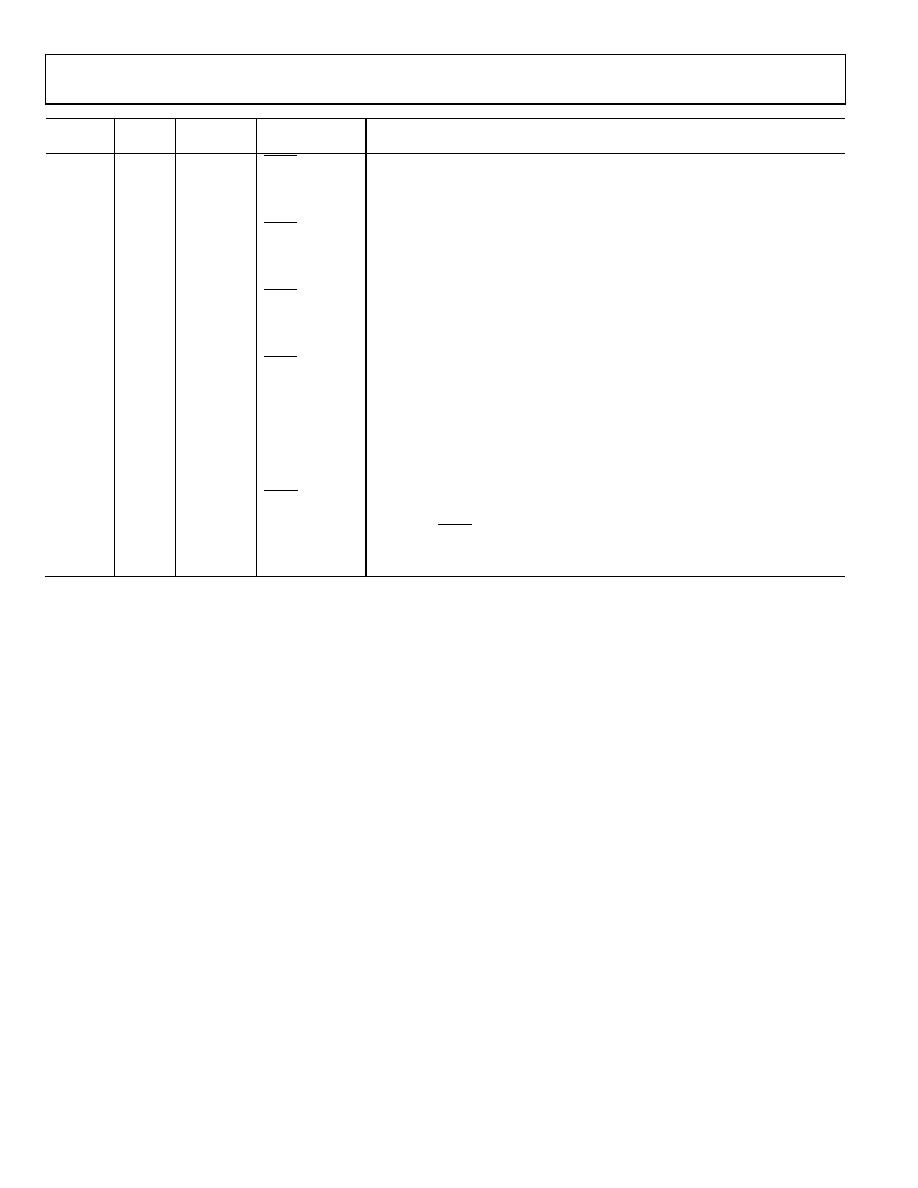
Pin No.
Input/
Output
Pin Type
Mnemonic
Description
47
O
LVPECL or
CMOS
OUT3 (OUT3B)
Clock Output. This pin can be configured as one side of a differential LVPECL output
or as a single-ended CMOS output.
48
O
LVPECL or
CMOS
OUT3 (OUT3A)
Clock Output. This pin can be configured as one side of a differential LVPECL output
or as a single-ended CMOS output.
50
O
LVPECL or
CMOS
OUT2 (OUT2B)
Clock Output. This pin can be configured as one side of a differential LVPECL output
or as a single-ended CMOS output.
51
O
LVPECL or
CMOS
OUT2 (OUT2A)
Clock Output. This pin can be configured as one side of a differential LVPECL output
or as a single-ended CMOS output.
52
O
LVPECL or
CMOS
OUT1 (OUT1B)
Clock Output. This pin can be configured as one side of a differential LVPECL output
or as a single-ended CMOS output.
53
O
LVPECL or
CMOS
OUT1 (OUT1A)
Clock Output. This pin can be configured as one side of a differential LVPECL output
or as a single-ended CMOS output.
55
O
LVPECL or
CMOS
OUT0 (OUT0B)
Clock Output. This pin can be configured as one side of a differential LVPECL output
or as a single-ended CMOS output.
56
O
LVPECL or
CMOS
OUT0 (OUT0A)
Clock Output. This pin can be configured as one side of a differential LVPECL output
or as a single-ended CMOS output.
58
O
Current set
resistor
RSET
Clock Distribution Current Set Resistor. Connect a 4.12 k resistor from this pin to GND.
62
O
Current set
resistor
CPRSET
Charge Pump Current Set Resistor. Connect a 5.1 k resistor from this pin to GND.
This resistor can be omitted if the PLL is not used.
63
I
Reference
input
REFIN (REF2)
Along with REFIN, this is the differential input for the PLL reference.
Alternatively, this pin is a single-ended input for REF2.
64
I
Reference
input
REFIN (REF1)
Along with REFIN, this is the differential input for the PLL reference.
Alternatively, this pin is a single-ended input for REF1.
EPAD
GND
The exposed die pad must be connected to GND.
相关PDF资料 |
PDF描述 |
|---|---|
| SRR4018-270Y | INDUCTOR POWER 27UH 0.77A 4018 |
| MLF2012E8R2K | INDUCTOR MULTILAYER 8.2UH 0805 |
| V110B48E150BL | CONVERTER MOD DC/DC 48V 150W |
| AD9515/PCBZ | BOARD EVAL CLOCK 2CH AD9515 |
| ECC30DCAN | CONN EDGECARD 60POS R/A .100 SLD |
相关代理商/技术参数 |
参数描述 |
|---|---|
| AD9520-1 | 制造商:AD 制造商全称:Analog Devices 功能描述:12 LVPECL/24 CMOS Output Clock Generator with Integrated 2.5 GHz VCO |
| AD9520-1/PCBZ | 功能描述:BOARD EVAL FOR AD9520-1 RoHS:是 类别:编程器,开发系统 >> 评估演示板和套件 系列:- 标准包装:1 系列:PSoC® 主要目的:电源管理,热管理 嵌入式:- 已用 IC / 零件:- 主要属性:- 次要属性:- 已供物品:板,CD,电源 |
| AD9520-1BCPZ | 功能描述:IC CLOCK GEN 2.5GHZ VCO 64LFCSP RoHS:是 类别:集成电路 (IC) >> 时钟/计时 - 时钟发生器,PLL,频率合成器 系列:- 标准包装:2,000 系列:- 类型:PLL 时钟发生器 PLL:带旁路 输入:LVCMOS,LVPECL 输出:LVCMOS 电路数:1 比率 - 输入:输出:2:11 差分 - 输入:输出:是/无 频率 - 最大:240MHz 除法器/乘法器:是/无 电源电压:3.135 V ~ 3.465 V 工作温度:0°C ~ 70°C 安装类型:表面贴装 封装/外壳:32-LQFP 供应商设备封装:32-TQFP(7x7) 包装:带卷 (TR) |
| AD9520-1BCPZ-REEL7 | 功能描述:IC CLOCK GEN 2.5GHZ VCO 64LFCSP RoHS:是 类别:集成电路 (IC) >> 时钟/计时 - 时钟发生器,PLL,频率合成器 系列:- 标准包装:2,000 系列:- 类型:PLL 时钟发生器 PLL:带旁路 输入:LVCMOS,LVPECL 输出:LVCMOS 电路数:1 比率 - 输入:输出:2:11 差分 - 输入:输出:是/无 频率 - 最大:240MHz 除法器/乘法器:是/无 电源电压:3.135 V ~ 3.465 V 工作温度:0°C ~ 70°C 安装类型:表面贴装 封装/外壳:32-LQFP 供应商设备封装:32-TQFP(7x7) 包装:带卷 (TR) |
| AD9520-2 | 制造商:AD 制造商全称:Analog Devices 功能描述:12 LVPECL/24 CMOS Output Clock Generator with Integrated 2.2 GHz VCO |
发布紧急采购,3分钟左右您将得到回复。