- 您现在的位置:买卖IC网 > PDF目录9093 > AD9571ACPZLVD-R7 (Analog Devices Inc)IC PLL CLOCK GEN 25MHZ 40LFCSP PDF资料下载
参数资料
| 型号: | AD9571ACPZLVD-R7 |
| 厂商: | Analog Devices Inc |
| 文件页数: | 8/20页 |
| 文件大小: | 0K |
| 描述: | IC PLL CLOCK GEN 25MHZ 40LFCSP |
| 标准包装: | 750 |
| 类型: | 时钟发生器,扇出配送,多路复用器 |
| PLL: | 是 |
| 输入: | 晶体 |
| 输出: | CMOS,LVDS,LVPECL |
| 电路数: | 1 |
| 比率 - 输入:输出: | 1:10 |
| 差分 - 输入:输出: | 无/是 |
| 频率 - 最大: | 156.25MHz |
| 除法器/乘法器: | 是/无 |
| 电源电压: | 2.97 V ~ 3.63 V |
| 工作温度: | -40°C ~ 85°C |
| 安装类型: | 表面贴装 |
| 封装/外壳: | 40-WFQFN 裸露焊盘,CSP |
| 供应商设备封装: | 40-LFCSP-WQ(6x6) |
| 包装: | 带卷 (TR) |
AD9571
Rev. 0 | Page 16 of 20
The value of the resistor is dependent on the board design and
timing requirements (typically 10 to 100 is used). CMOS
outputs are limited in terms of the capacitive load or trace
length that they can drive. Typically, trace lengths less than
6 inches are recommended to preserve signal rise/fall times
and signal integrity.
10
MICROSTRIP
GND
5pF
60.4
1.0 INCH
CMOS
07499-
015
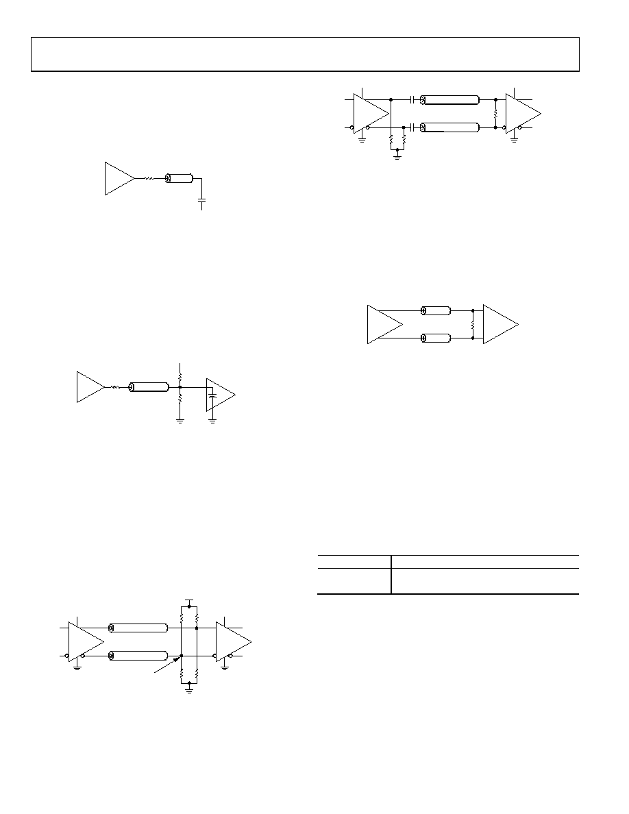
Figure 15. Series Termination of CMOS Output
Termination at the far end of the PCB trace is a second option.
The CMOS outputs of the AD9571 do not supply enough current
to provide a full voltage swing with a low impedance resistive,
far-end termination, as shown in Figure 16. The far-end termin-
ation network should match the PCB trace impedance and
provide the desired switching point. The reduced signal swing
may still meet receiver input requirements in some applications.
This can be useful when driving long trace lengths on less
critical nets.
50
10
VPULLUP = 3.3V
CMOS
5pF
100
100
07499-
016
Figure 16. CMOS Output with Far-End Termination
LVPECL CLOCK DISTRIBUTION
The low voltage, positive emitter-coupled logic (LVPECL)
outputs of the AD9571 provide the lowest jitter clock signals
available from the AD9571. The LVPECL outputs (because they
are open emitter) require a dc termination to bias the output
transistors. The simplified equivalent circuit in Figure 13 shows
the LVPECL output stage.
In most applications, a standard LVPECL far-end termination is
recommended, as shown in Figure 17. The resistor network is
designed to match the transmission line impedance (50) and
the desired switching threshold (1.3 V).
3.3V
LVPECL
50
50
SINGLE-ENDED
(NOT COUPLED)
3.3V
LVPECL
127
127
83
83
VT = VCC – 1.3V
07499-
017
Figure 17. LVPECL Far-End Termination
3.3V
LVPECL
DIFFERENTIAL
(COUPLED)
3.3V
LVPECL
100
0.1nF
200
200
07499-
018
Figure 18. LVPECL with Parallel Transmission Line
LVDS CLOCK DISTRIBUTION
Low voltage differential signaling (LVDS) is a second differ-
ential output option for the AD9571. LVDS uses a current mode
output stage with a factory programmed current level. The
normal value (default) for this current is 3.5 mA, which yields a
350 mV output swing across a 100 resistor. The LVDS
outputs meet or exceed all ANSI/TIA/EIA-644 specifications.
A recommended termination circuit for the LVDS outputs is
shown in Figure 19.
50
50
LVDS
100
07499-
019
Figure 19. LVDS Output Termination
See the AN-586 Application Note on the Analog Devices
website at www.analog.com for more information about LVDS.
REFERENCE INPUT
By default, the crystal oscillator is enabled and used as the
reference source, which requires the connection of an external
25 MHz crystal. The REFSEL pin is pulled high internally by
about 30 kΩ to support default operation. When REFSEL is tied
low, the crystal oscillator is powered down, and the REFCLK pin
must provide a good quality 25 MHz reference clock instead.
This single-ended input can be driven by either a dc-coupled
LVCMOS level signal or an ac-coupled sine wave or square
wave, provided that an external divider is used to bias the input
at VS/2.
Table 17. REFSEL Definition
REFSEL
Reference Source
0
REFCLK input
1
Internal crystal oscillator
POWER AND GROUNDING CONSIDERATIONS AND
POWER SUPPLY REJECTION
Many applications seek high speed and performance under
less than ideal operating conditions. In these application
circuits, the implementation and construction of the PCB is as
important as the circuit design. Proper RF techniques must be
used for device selection, placement, and routing, as well as for
power supply bypassing and grounding to ensure optimum
performance.
相关PDF资料 |
PDF描述 |
|---|---|
| SY10EL38LZG | IC CLK GEN /2 /4/6 3.3/5V 20SOIC |
| VE-2T3-IV | CONVERTER MOD DC/DC 24V 150W |
| VE-2T3-MW-S | CONVERTER MOD DC/DC 24V 100W |
| VI-25P-MW-S | CONVERTER MOD DC/DC 13.8V 100W |
| AD9572ACPZPEC-R7 | IC PLL CLOCK GEN 25MHZ 40LFCSP |
相关代理商/技术参数 |
参数描述 |
|---|---|
| AD9571ACPZLVD-RL | 功能描述:IC PLL CLOCK GEN 25MHZ 40LFCSP RoHS:是 类别:集成电路 (IC) >> 时钟/计时 - 时钟发生器,PLL,频率合成器 系列:- 标准包装:1,000 系列:Precision Edge® 类型:时钟/频率合成器 PLL:无 输入:CML,PECL 输出:CML 电路数:1 比率 - 输入:输出:2:1 差分 - 输入:输出:是/是 频率 - 最大:10.7GHz 除法器/乘法器:无/无 电源电压:2.375 V ~ 3.6 V 工作温度:-40°C ~ 85°C 安装类型:表面贴装 封装/外壳:16-VFQFN 裸露焊盘,16-MLF? 供应商设备封装:16-MLF?(3x3) 包装:带卷 (TR) 其它名称:SY58052UMGTRSY58052UMGTR-ND |
| AD9571ACPZPEC | 功能描述:IC PLL CLOCK GEN 25MHZ 40LFCSP RoHS:是 类别:集成电路 (IC) >> 时钟/计时 - 时钟发生器,PLL,频率合成器 系列:- 标准包装:2,000 系列:- 类型:PLL 频率合成器 PLL:是 输入:晶体 输出:时钟 电路数:1 比率 - 输入:输出:1:1 差分 - 输入:输出:无/无 频率 - 最大:1GHz 除法器/乘法器:是/无 电源电压:4.5 V ~ 5.5 V 工作温度:-20°C ~ 85°C 安装类型:表面贴装 封装/外壳:16-LSSOP(0.175",4.40mm 宽) 供应商设备封装:16-SSOP 包装:带卷 (TR) 其它名称:NJW1504V-TE1-NDNJW1504V-TE1TR |
| AD9571ACPZPEC-R7 | 功能描述:IC PLL CLOCK GEN 25MHZ 40LFCSP RoHS:是 类别:集成电路 (IC) >> 时钟/计时 - 时钟发生器,PLL,频率合成器 系列:- 标准包装:1,000 系列:Precision Edge® 类型:时钟/频率合成器 PLL:无 输入:CML,PECL 输出:CML 电路数:1 比率 - 输入:输出:2:1 差分 - 输入:输出:是/是 频率 - 最大:10.7GHz 除法器/乘法器:无/无 电源电压:2.375 V ~ 3.6 V 工作温度:-40°C ~ 85°C 安装类型:表面贴装 封装/外壳:16-VFQFN 裸露焊盘,16-MLF? 供应商设备封装:16-MLF?(3x3) 包装:带卷 (TR) 其它名称:SY58052UMGTRSY58052UMGTR-ND |
| AD9571ACPZPEC-RL | 功能描述:IC PLL CLOCK GEN 25MHZ 40LFCSP RoHS:是 类别:集成电路 (IC) >> 时钟/计时 - 时钟发生器,PLL,频率合成器 系列:- 标准包装:1,000 系列:Precision Edge® 类型:时钟/频率合成器 PLL:无 输入:CML,PECL 输出:CML 电路数:1 比率 - 输入:输出:2:1 差分 - 输入:输出:是/是 频率 - 最大:10.7GHz 除法器/乘法器:无/无 电源电压:2.375 V ~ 3.6 V 工作温度:-40°C ~ 85°C 安装类型:表面贴装 封装/外壳:16-VFQFN 裸露焊盘,16-MLF? 供应商设备封装:16-MLF?(3x3) 包装:带卷 (TR) 其它名称:SY58052UMGTRSY58052UMGTR-ND |
| AD9572 | 制造商:AD 制造商全称:Analog Devices 功能描述:Fiber Channel/Ethernet Clock Generator IC, PLL Core, Dividers, 7 Clock Outputs |
发布紧急采购,3分钟左右您将得到回复。