- 您现在的位置:买卖IC网 > PDF目录1987 > AD9573ARUZ-RL7 (Analog Devices Inc)IC PCI CLCOK GEN 25MHZ 16TSSOP PDF资料下载
参数资料
| 型号: | AD9573ARUZ-RL7 |
| 厂商: | Analog Devices Inc |
| 文件页数: | 2/12页 |
| 文件大小: | 0K |
| 描述: | IC PCI CLCOK GEN 25MHZ 16TSSOP |
| 标准包装: | 1,000 |
| 系列: | PCI Express® (PCIe) |
| 类型: | 时钟/频率发生器,扇出缓冲器(分配) |
| PLL: | 是 |
| 主要目的: | PCI Express(PCIe) |
| 输入: | 晶体 |
| 输出: | LVCMOS,LVDS |
| 电路数: | 1 |
| 比率 - 输入:输出: | 1:2 |
| 差分 - 输入:输出: | 无/是 |
| 频率 - 最大: | 100MHz |
| 电源电压: | 3 V ~ 3.6 V |
| 工作温度: | -40°C ~ 85°C |
| 安装类型: | 表面贴装 |
| 封装/外壳: | 16-TSSOP(0.173",4.40mm 宽) |
| 供应商设备封装: | 16-TSSOP |
| 包装: | 带卷 (TR) |
AD9573
Rev. 0 | Page 10 of 12
evaluation board shows a good example (see the Ordering
Guide for information about the evaluation board).
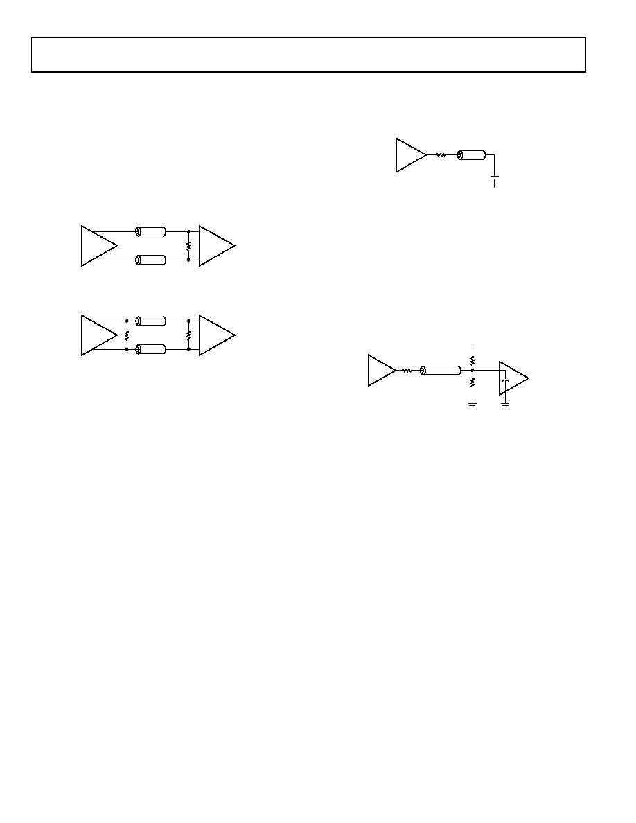
LVDS CLOCK DISTRIBUTION
Low voltage differential signaling (LVDS) is the differential
output for the AD9573. LVDS uses a current mode output stage
with a factory programmed current level. The normal value
(default) for this current is 6.5 mA, which yields a 650 mV
output swing across a 100 Ω resistor.
The typical termination circuit for the LVDS outputs is shown
in Figure 11.
50
LVDS
100
0
75
00
-01
4
Figure 11. LVDS Output Termination
An alternative method of terminating the output to preserve output
swing but also minimize reflections is shown in Figure 12.
50
LVDS
200
0
75
00
-01
5
Figure 12. Alternative LVDS Output Termination
CMOS CLOCK DISTRIBUTION
The AD9573 provides a 33.33 MHz clock output, which is a
dedicated CMOS level. Whenever single-ended CMOS clocking
is used, some of the following general guidelines should be
followed.
Point-to-point nets should be designed such that a driver has
one receiver only on the net, if possible. This allows for simple
termination schemes and minimizes ringing due to possible
mismatched impedances on the net. Series termination at the
source is generally required to provide transmission line
matching and/or to reduce current transients at the driver. The
value of the resistor is dependent on the board design and
timing requirements (typically 10 Ω to 100 Ω is used). CMOS
outputs are limited in terms of the capacitive load or trace
length that they can drive. Typically, trace lengths less than
6 inches are recommended to preserve signal rise/fall times
and preserve signal integrity.
10
MICROSTRIP
GND
5pF
60.4
1.0 INCH
CMOS
0
75
00
-01
6
Figure 13. Series Termination of CMOS Output
Termination at the far end of the PCB trace is a second option.
The CMOS output of the AD9573 does not supply enough
current to provide a full voltage swing with a low impedance
resistive, far end termination, as shown in Figure 14. The far
end termination network should match the PCB trace
impedance and provide the desired switching point.
The reduced signal swing may still meet receiver input require-
ments in some applications. This can be useful when driving
long trace lengths on less critical nets.
VPULLUP = 3.3V
50
10
CMOS
3pF
100
0
75
00
-0
17
Figure 14. CMOS Output with Far-End Termination
POWER AND GROUNDING CONSIDERATIONS AND
POWER SUPPLY REJECTION
Many applications seek high speed and performance under
less than ideal operating conditions. In these application
circuits, the implementation and construction of the PCB is as
important as the circuit design. Proper RF techniques must be
used for device selection, placement, and routing, as well as for
power supply decoupling and grounding to ensure optimum
performance.
相关PDF资料 |
PDF描述 |
|---|---|
| AD9575ARUZPEC | IC PLL CLOCK GEN 25MHZ 16TSSOP |
| AD9577BCPZ-R7 | IC CLOCK GENERATOR 40LFCSP |
| AD9600ABCPZ-150 | IC ADC 10BIT 150MSPS 64LFCSP |
| AD9608BCPZRL7-125 | IC ADC 10BIT 125MSPS 64LFCSP |
| AD9609BCPZRL7-80 | IC ADC 10BIT SRL/SPI 80M 32LFCSP |
相关代理商/技术参数 |
参数描述 |
|---|---|
| AD9573-EVALZ | 制造商:AD 制造商全称:Analog Devices 功能描述:PCI-Express Clock Generator IC, PLL Core, Dividers, Two Outputs |
| AD9574BCPZ | 功能描述:IC PLL CLOCK GEN 25MHZ 制造商:analog devices inc. 系列:- 包装:托盘 零件状态:有效 类型:* PLL:带旁路 输入:时钟 输出:CMOS,HCSL,HSTL,LVDS 电路数:1 比率 - 输入:输出:2:7 差分 - 输入:输出:是/是 频率 - 最大值:312.5MHz 分频器/倍频器:是/是 电压 - 电源:2.97 V ~ 3.63 V 工作温度:-40°C ~ 85°C 安装类型:表面贴装 封装/外壳:48-WFQFN 裸露焊盘,CSP 供应商器件封装:48-LFCSP-WQ(7x7) 标准包装:1 |
| AD9574BCPZ-REEL7 | 功能描述:IC PLL CLOCK GEN 25MHZ 制造商:analog devices inc. 系列:- 包装:带卷(TR) 零件状态:有效 类型:* PLL:带旁路 输入:时钟 输出:CMOS,HCSL,HSTL,LVDS 电路数:1 比率 - 输入:输出:2:7 差分 - 输入:输出:是/是 频率 - 最大值:312.5MHz 分频器/倍频器:是/是 电压 - 电源:2.97 V ~ 3.63 V 工作温度:-40°C ~ 85°C 安装类型:表面贴装 封装/外壳:48-WFQFN 裸露焊盘,CSP 供应商器件封装:48-LFCSP-WQ(7x7) 标准包装:750 |
| AD9575 | 制造商:AD 制造商全称:Analog Devices 功能描述:Network Clock Generator, Two Outputs |
| AD9575ARUZLVD | 功能描述:IC PLL CLOCK GEN 25MHZ 16TSSOP RoHS:是 类别:集成电路 (IC) >> 时钟/计时 - 专用 系列:PCI Express® (PCIe) 标准包装:28 系列:- 类型:时钟/频率发生器 PLL:是 主要目的:Intel CPU 服务器 输入:时钟 输出:LVCMOS 电路数:1 比率 - 输入:输出:3:22 差分 - 输入:输出:无/是 频率 - 最大:400MHz 电源电压:3.135 V ~ 3.465 V 工作温度:0°C ~ 85°C 安装类型:表面贴装 封装/外壳:64-TFSOP (0.240",6.10mm 宽) 供应商设备封装:64-TSSOP 包装:管件 |
发布紧急采购,3分钟左右您将得到回复。