- 您现在的位置:买卖IC网 > PDF目录17025 > AD9609-40EBZ (Analog Devices Inc)BOARD EVALUATION AD9609 40MSPS PDF资料下载
参数资料
| 型号: | AD9609-40EBZ |
| 厂商: | Analog Devices Inc |
| 文件页数: | 9/32页 |
| 文件大小: | 0K |
| 描述: | BOARD EVALUATION AD9609 40MSPS |
| 设计资源: | AD9649/29/09 Schematics AD9649/29/09 Gerber Files |
| 标准包装: | 1 |
| ADC 的数量: | 1 |
| 位数: | 10 |
| 采样率(每秒): | 40M |
| 数据接口: | 串行,SPI? |
| 输入范围: | 2 Vpp |
| 在以下条件下的电源(标准): | 57.4mW @ 40MSPS |
| 工作温度: | -40°C ~ 85°C |
| 已用 IC / 零件: | AD9609 |
| 已供物品: | 板 |
第1页第2页第3页第4页第5页第6页第7页第8页当前第9页第10页第11页第12页第13页第14页第15页第16页第17页第18页第19页第20页第21页第22页第23页第24页第25页第26页第27页第28页第29页第30页第31页第32页
AD9609
Rev. 0 | Page 17 of 32
THEORY OF OPERATION
The AD9609 architecture consists of a multistage, pipelined ADC.
Each stage provides sufficient overlap to correct for flash errors in
the preceding stage. The quantized outputs from each stage are
combined into a final 10-bit result in the digital correction logic.
The pipelined architecture permits the first stage to operate with a
new input sample while the remaining stages operate with pre-
ceding samples. Sampling occurs on the rising edge of the clock.
Each stage of the pipeline, excluding the last, consists of a low
resolution flash ADC connected to a switched-capacitor DAC
and an interstage residue amplifier (for example, a multiplying
digital-to-analog converter (MDAC)). The residue amplifier
magnifies the difference between the reconstructed DAC output
and the flash input for the next stage in the pipeline. One bit of
redundancy is used in each stage to facilitate digital correction
of flash errors. The last stage simply consists of a flash ADC.
The output staging block aligns the data, corrects errors, and
passes the data to the CMOS output buffers. The output buffers
are powered from a separate (DRVDD) supply, allowing adjust-
ment of the output voltage swing. During power-down, the
output buffers go into a high impedance state.
ANALOG INPUT CONSIDERATIONS
The analog input to the AD9609 is a differential switched-
capacitor circuit designed for processing differential input
signals. This circuit can support a wide common-mode range
while maintaining excellent performance. By using an input
common-mode voltage of midsupply, users can minimize
signal-dependent errors and achieve optimum performance.
SS
H
CPAR
CSAMPLE
CPAR
VIN–
H
SS
H
VIN+
H
08
54
1-
0
06
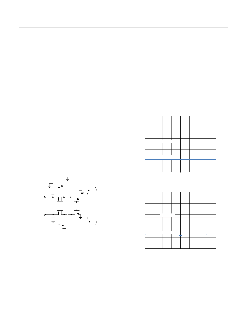
Figure 34. Switched-Capacitor Input Circuit
The clock signal alternately switches the input circuit between
sample-and-hold mode (see Figure 34). When the input circuit
is switched to sample mode, the signal source must be capable
of charging the sample capacitors and settling within one-half
of a clock cycle. A small resistor in series with each input can
help reduce the peak transient current injected from the output
stage of the driving source. In addition, low Q inductors or ferrite
beads can be placed on each leg of the input to reduce high diffe-
rential capacitance at the analog inputs and, therefore, achieve
the maximum bandwidth of the ADC. Such use of low Q inductors
or ferrite beads is required when driving the converter front end at
high IF frequencies. Either a shunt capacitor or two single-ended
capacitors can be placed on the inputs to provide a matching
passive network. This ultimately creates a low-pass filter at the
input to limit unwanted broadband noise. See the AN-742
Application Note, the AN-827 Application Note, and the Analog
Dialogue article “Transformer-Coupled Front-End for Wideband
A/D Converters” (Volume 39, April 2005) for more information. In
general, the precise values depend on the application.
Input Common Mode
The analog inputs of the AD9609 are not internally dc-biased.
Therefore, in ac-coupled applications, the user must provide a
dc bias externally. Setting the device so that VCM = AVDD/2 is
recommended for optimum performance, but the device can
function over a wider range with reasonable performance, as
50
60
70
80
90
100
0.5
0.6
0.7
0.8
0.9
1.0
1.1
1.2
1.3
S
NR/
S
F
DR
(
d
BF
S
/d
B
c)
INPUT COMMON-MODE VOLTAGE (V)
SFDR (dBc)
SNR (dBFS)
0
85
41
-1
39
Figure 35. SNR/SFDR vs. Input Common-Mode Voltage,
fIN = 32.1 MHz, fS = 80 MSPS
50
60
70
80
90
100
0.50.60.70.80.91.0
1.11.21.3
S
NR/
S
F
DR
(
d
BF
S
/d
B
c)
INPUT COMMON-MODE VOLTAGE (V)
SFDR (dBc)
SNR (dBFS)
0
85
41
-1
40
Figure 36. SNR/SFDR vs. Input Common-Mode Voltage,
fIN = 10.3 MHz, fS = 20 MSPS
An on-board, common-mode voltage reference is included in
the design and is available from the VCM pin. The VCM pin
must be decoupled to ground by a 0.1 μF capacitor, as described
in the Applications Information section.
相关PDF资料 |
PDF描述 |
|---|---|
| EEM36DRXS | CONN EDGECARD 72POS DIP .156 SLD |
| EBM28DRUI | CONN EDGECARD 56POS DIP .156 SLD |
| SI3865CDV-T1-E3 | IC LOAD SWITCH LVL SHIFT 6-TSOP |
| EBM22DRTF | CONN EDGECARD 44POS DIP .156 SLD |
| 0982660817 | CBL 13POS 0.5MM JMPR TYPE A 4" |
相关代理商/技术参数 |
参数描述 |
|---|---|
| AD9609-65EBZ | 功能描述:BOARD EVALUATION AD9609 65MSPS RoHS:是 类别:编程器,开发系统 >> 评估板 - 模数转换器 (ADC) 系列:- 产品培训模块:Obsolescence Mitigation Program 标准包装:1 系列:- ADC 的数量:1 位数:12 采样率(每秒):94.4k 数据接口:USB 输入范围:±VREF/2 在以下条件下的电源(标准):- 工作温度:-40°C ~ 85°C 已用 IC / 零件:MAX11645 已供物品:板,软件 |
| AD9609-80EBZ | 功能描述:BOARD EVALUATION AD9609 80MSPS RoHS:是 类别:编程器,开发系统 >> 评估板 - 模数转换器 (ADC) 系列:- 产品培训模块:Obsolescence Mitigation Program 标准包装:1 系列:- ADC 的数量:1 位数:12 采样率(每秒):94.4k 数据接口:USB 输入范围:±VREF/2 在以下条件下的电源(标准):- 工作温度:-40°C ~ 85°C 已用 IC / 零件:MAX11645 已供物品:板,软件 |
| AD9609BCPZ-20 | 功能描述:IC ADC 10BIT 20MSPS LP 32LFCSP RoHS:是 类别:集成电路 (IC) >> 数据采集 - 模数转换器 系列:- 标准包装:1 系列:microPOWER™ 位数:8 采样率(每秒):1M 数据接口:串行,SPI? 转换器数目:1 功率耗散(最大):- 电压电源:模拟和数字 工作温度:-40°C ~ 125°C 安装类型:表面贴装 封装/外壳:24-VFQFN 裸露焊盘 供应商设备封装:24-VQFN 裸露焊盘(4x4) 包装:Digi-Reel® 输入数目和类型:8 个单端,单极 产品目录页面:892 (CN2011-ZH PDF) 其它名称:296-25851-6 |
| AD9609BCPZ-40 | 功能描述:IC ADC 10BIT 40MSPS LP 32LFCSP RoHS:是 类别:集成电路 (IC) >> 数据采集 - 模数转换器 系列:- 标准包装:1 系列:microPOWER™ 位数:8 采样率(每秒):1M 数据接口:串行,SPI? 转换器数目:1 功率耗散(最大):- 电压电源:模拟和数字 工作温度:-40°C ~ 125°C 安装类型:表面贴装 封装/外壳:24-VFQFN 裸露焊盘 供应商设备封装:24-VQFN 裸露焊盘(4x4) 包装:Digi-Reel® 输入数目和类型:8 个单端,单极 产品目录页面:892 (CN2011-ZH PDF) 其它名称:296-25851-6 |
| AD9609BCPZ-65 | 功能描述:IC ADC 10BIT 65MSPS LP 32LFCSP RoHS:是 类别:集成电路 (IC) >> 数据采集 - 模数转换器 系列:- 标准包装:1 系列:microPOWER™ 位数:8 采样率(每秒):1M 数据接口:串行,SPI? 转换器数目:1 功率耗散(最大):- 电压电源:模拟和数字 工作温度:-40°C ~ 125°C 安装类型:表面贴装 封装/外壳:24-VFQFN 裸露焊盘 供应商设备封装:24-VQFN 裸露焊盘(4x4) 包装:Digi-Reel® 输入数目和类型:8 个单端,单极 产品目录页面:892 (CN2011-ZH PDF) 其它名称:296-25851-6 |
发布紧急采购,3分钟左右您将得到回复。