- 您现在的位置:买卖IC网 > PDF目录10527 > AD9634BCPZ-170 (Analog Devices Inc)IC ADC 12BIT 170MSPS 32-LFCSP PDF资料下载
参数资料
| 型号: | AD9634BCPZ-170 |
| 厂商: | Analog Devices Inc |
| 文件页数: | 14/32页 |
| 文件大小: | 0K |
| 描述: | IC ADC 12BIT 170MSPS 32-LFCSP |
| 标准包装: | 1 |
| 位数: | 12 |
| 采样率(每秒): | 170M |
| 数据接口: | 串行,SPI? |
| 转换器数目: | 1 |
| 功率耗散(最大): | 340mW |
| 电压电源: | 模拟和数字 |
| 工作温度: | -40°C ~ 85°C |
| 安装类型: | 表面贴装 |
| 封装/外壳: | 32-WFQFN 裸露焊盘,CSP |
| 供应商设备封装: | 32-LFCSP-WQ(5x5) |
| 包装: | 托盘 |
| 输入数目和类型: | 2 单端,1 个差分 |
第1页第2页第3页第4页第5页第6页第7页第8页第9页第10页第11页第12页第13页当前第14页第15页第16页第17页第18页第19页第20页第21页第22页第23页第24页第25页第26页第27页第28页第29页第30页第31页第32页
AD9634
Rev. 0 | Page 21 of 32
AD8375
AD9634
1H
1nF
VPOS
VCM
15pF
68nH
2.5k║2pF
301
165
5.1pF
3.9pF
180nH
1000pF
1000pF 180nH
220nH
NOTES
1. ALL INDUCTORS ARE COILCRAFT 0603CS COMPONENTS
WITH THE EXCEPTION OF THE 1H CHOKE INDUCTORS (0603LS).
2. FILTER VALUES SHOWN ARE FOR A 20MHz BANDWIDTH FILTER CENTERED AT 140MHz.
099
96-
0
47
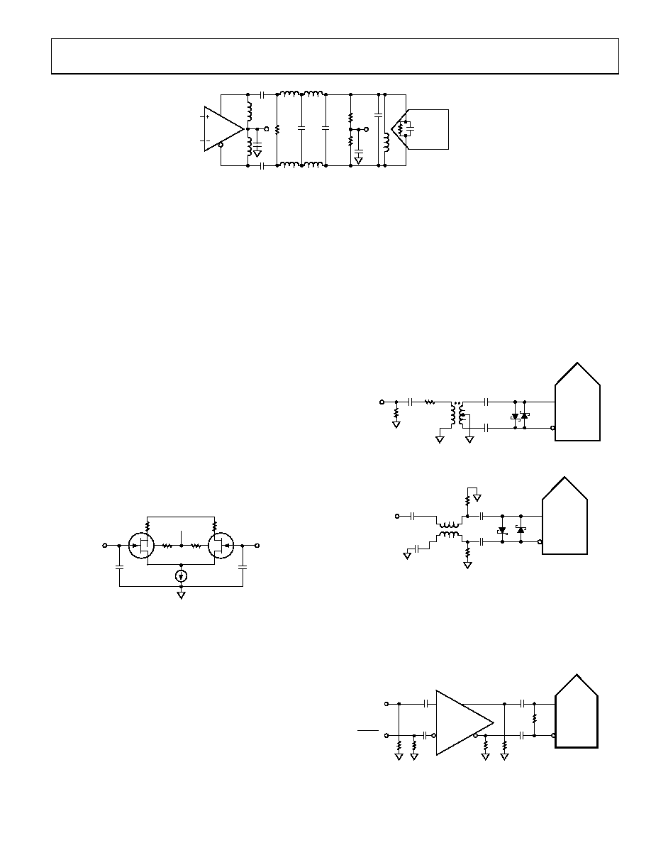
Figure 50. Differential Input Configuration Using the AD8375
An alternative to using a transformer-coupled input at
frequencies in the second Nyquist zone is to use an amplifier
with variable gain. The AD8375 digital variable gain amplifier
(DVGA) provides good performance for driving the AD9634.
through a band-pass antialiasing filter.
VOLTAGE REFERENCE
A stable and accurate voltage reference is built into the AD9634.
The full-scale input range can be adjusted by varying the reference
voltage via SPI. The input span of the ADC tracks reference
voltage changes linearly.
CLOCK INPUT CONSIDERATIONS
For optimum performance, the AD9634 sample clock inputs,
CLK+ and CLK, should be clocked with a differential signal.
The signal is typically ac-coupled into the CLK+ and CLK pins by
means of a transformer or a passive component configuration.
These pins are biased internally (see Figure 51) and require no
external bias. If the inputs are floated, the CLK pin is pulled low
to prevent spurious clocking.
AVDD
CLK+
4pF
CLK–
0.9V
09
99
6-
0
48
Figure 51. Equivalent Clock Input Circuit
Clock Input Options
The AD9634 has a very flexible clock input structure. Clock input
can be a CMOS, LVDS, LVPECL, or sine wave signal. Regardless
of the type of signal being used, clock source jitter is of the most
concern, as described in the Jitter Considerations section.
the AD9634 (at clock rates of up to 625 MHz). A low jitter clock
source is converted from a single-ended signal to a differential
signal using an RF balun or RF transformer.
The RF balun configuration is recommended for clock frequencies
between 125 MHz and 625 MHz, and the RF transformer is
recommended for clock frequencies from 10 MHz to 200 MHz.
The back-to-back Schottky diodes across the secondary windings
of the transformer limit clock excursions into the AD9634 to
approximately 0.8 V p-p differential. This limit helps prevent the
large voltage swings of the clock from feeding through to other
portions of the AD9634, while preserving the fast rise and fall times
of the signal, which are critical for low jitter performance.
390pF
SCHOTTKY
DIODES:
HSMS2822
CLOCK
INPUT
50
100
CLK–
CLK+
ADC
Mini-Circuits
ADT1-1WT, 1:1Z
XFMR
09
996-
05
6
Figure 52. Transformer Coupled Differential Clock (Up to 200 MHz)
390pF
CLOCK
INPUT
1nF
25
CLK–
CLK+
SCHOTTKY
DIODES:
HSMS2822
ADC
0
999
6-
0
57
Figure 53. Balun-Coupled Differential Clock (Up to 625 MHz)
If a low jitter clock source is not available, another option is to
ac couple a differential PECL signal to the sample clock input pins
clock drivers offer excellent jitter performance.
100
0.1F
240
PECL DRIVER
50k
CLK–
CLK+
CLOCK
INPUT
CLOCK
INPUT
AD95xx,
ADCLKxxx
ADC
09
996
-0
51
Figure 54. Differential PECL Sample Clock (Up to 625 MHz)
相关PDF资料 |
PDF描述 |
|---|---|
| DS34LV87TM/NOPB | IC LINE DRIVER QUAD CMOS 16-SOIC |
| AD7711ANZ | IC ADC 24BIT RTD I SOURCE 24-DIP |
| AD9600ABCPZ-125 | IC ADC 10BIT 125MSPS 64LFCSP |
| ICL3237CAZ | IC 5DRVR/3RCVR RS232 3V 28-SSOP |
| AMIS42665TJAA1G | TRANSCEIVER CAN HS LP 8-SOIC |
相关代理商/技术参数 |
参数描述 |
|---|---|
| AD9634BCPZ-210 | 制造商:Analog Devices 功能描述:12 BIT 210 MSPS ADC - Trays 制造商:Analog Devices 功能描述:IC ADC 12BIT 210MSPS 32-LFCSP 制造商:Analog Devices 功能描述:ADC 12BIT 210MSPS 32LFCSP 制造商:Analog Devices 功能描述:IC ADC 12 bit 210 MSPS Ser 制造商:Analog Devices 功能描述:ADC, 12BIT, 210MSPS, 32LFCSP 制造商:Analog Devices 功能描述:12 Bit 210 Msps ADC 制造商:Analog Devices 功能描述:CONVERTER - ADC |
| AD9634BCPZ-250 | 制造商:Analog Devices 功能描述:12 BIT 250 MSPS ADC - Trays 制造商:Analog Devices 功能描述:IC ADC 12BIT 250MSPS 32-LFCSP 制造商:Analog Devices 功能描述:IC ADC 12 bit 250 MSPS Ser 制造商:Analog Devices 功能描述:ADC 12BIT 250MSPS 32LFCSP 制造商:Analog Devices 功能描述:ADC, 12BIT, 250MSPS, 32LFCSP 制造商:Analog Devices 功能描述:12 Bit 250 Msps ADC 制造商:Analog Devices 功能描述:CONVERTER - ADC |
| AD9634BCPZRL7-170 | 功能描述:IC ADC 12BIT SRL 170MSPS 32LFCSP RoHS:是 类别:集成电路 (IC) >> 数据采集 - 模数转换器 系列:- 标准包装:1 系列:- 位数:14 采样率(每秒):83k 数据接口:串行,并联 转换器数目:1 功率耗散(最大):95mW 电压电源:双 ± 工作温度:0°C ~ 70°C 安装类型:通孔 封装/外壳:28-DIP(0.600",15.24mm) 供应商设备封装:28-PDIP 包装:管件 输入数目和类型:1 个单端,双极 |
| AD9634BCPZRL7-210 | 功能描述:模数转换器 - ADC 12 Bit 210 Msps ADC RoHS:否 制造商:Analog Devices 通道数量: 结构: 转换速率: 分辨率: 输入类型: 信噪比: 接口类型: 工作电源电压: 最大工作温度: 安装风格: 封装 / 箱体: |
| AD9634BCPZRL7-250 | 功能描述:模数转换器 - ADC 12 Bit 250 Msps ADC RoHS:否 制造商:Analog Devices 通道数量: 结构: 转换速率: 分辨率: 输入类型: 信噪比: 接口类型: 工作电源电压: 最大工作温度: 安装风格: 封装 / 箱体: |
发布紧急采购,3分钟左右您将得到回复。