参数资料
| 型号: | AD9705BCPZ |
| 厂商: | Analog Devices Inc |
| 文件页数: | 24/44页 |
| 文件大小: | 0K |
| 描述: | IC DAC TX 10BIT 175MSPS 32-LFCSP |
| 产品培训模块: | Data Converter Fundamentals DAC Architectures |
| 标准包装: | 1 |
| 系列: | TxDAC® |
| 设置时间: | 11ns |
| 位数: | 10 |
| 数据接口: | 串行 |
| 转换器数目: | 1 |
| 电压电源: | 模拟和数字 |
| 功率耗散(最大): | 50mW |
| 工作温度: | -40°C ~ 85°C |
| 安装类型: | 表面贴装 |
| 封装/外壳: | 32-VFQFN 裸露焊盘,CSP |
| 供应商设备封装: | 32-LFCSP-VQ(5x5) |
| 包装: | 托盘 |
| 输出数目和类型: | 2 电流,单极 |
| 采样率(每秒): | 175M |
| 产品目录页面: | 785 (CN2011-ZH PDF) |
| 配用: | AD9705-EBZ-ND - BOARD EVAL FOR AD9705 |
第1页第2页第3页第4页第5页第6页第7页第8页第9页第10页第11页第12页第13页第14页第15页第16页第17页第18页第19页第20页第21页第22页第23页当前第24页第25页第26页第27页第28页第29页第30页第31页第32页第33页第34页第35页第36页第37页第38页第39页第40页第41页第42页第43页第44页
AD9704/AD9705/AD9706/AD9707
Data Sheet
Rev. B | Page 30 of 44
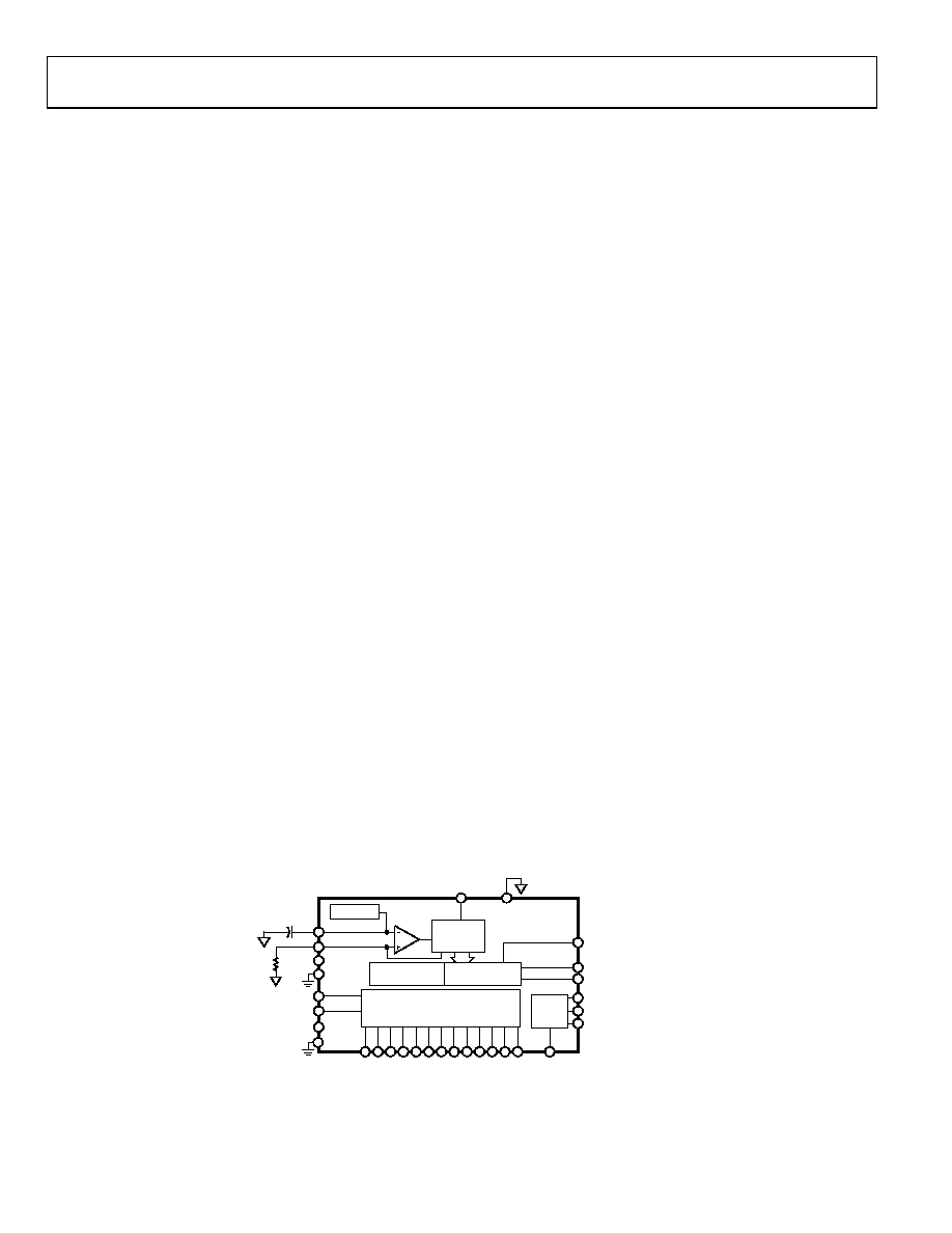
THEORY OF OPERATION
control logic, and full-scale output current control. The DAC
contains a PMOS current source array capable of providing a
nominal full-scale current (IOUTFS) of 2 mA and a maximum of
5 mA. The array is divided into 31 equal currents that make up the
five most significant bits (MSBs). The next four bits, or middle
bits, consist of 15 equal current sources whose value is 1/16 of an
MSB current source. The remaining LSBs are binary weighted frac-
tions of the current sources of the middle bits. Implementing the
middle and lower bits with current sources, instead of an R-2R
performance for multitone or low amplitude signals and helps
maintain the high output impedance of the DAC (that is,
>200 MΩ).
All of these current sources are switched to one of the two
output nodes (IOUTA or IOUTB) via PMOS differential current
switches. The switches are based on the architecture pioneered
in the AD9764 family, with further refinements made to reduce
distortion contributed by the switching transient. This switch
architecture also reduces various timing errors and provides
matching complementary drive signals to the inputs of the
differential current switches.
AD9707 have separate power supply inputs (AVDD and DVDD)
that can operate independently over a 1.7 V to 3.6 V range. The
digital section, capable of operating at a rate of up to 175 MSPS,
consists of edge-triggered latches and segment decoding logic
circuitry. The analog section includes the PMOS current
sources, the associated differential switches, a 1.0 V band gap
voltage reference, and a reference control amplifier.
The DAC full-scale output current is regulated by the reference
control amplifier and can be set from 1 mA to 5 mA via an external
resistor, RSET, connected to the full-scale adjust (FS ADJ) pin.
The external resistor, in combination with both the reference
control amplifier and voltage reference, VREFIO, sets the reference
current, IREF, which is replicated to the segmented current sources
with the proper scaling factor. The full-scale current, IOUTFS, is
32 × IREF.
setting the output common mode to a value other than ACOM
via the output common mode (OTCM) pin. This facilitates
directly to components that require common-mode levels greater
than 0 V.
SERIAL PERIPHERAL INTERFACE
synchronous serial communications port allowing easy interfacing
to many industry-standard microcontrollers and microprocessors.
The serial I/O is compatible with most synchronous transfer
formats, including the Motorola SPI and Intel SSR protocols.
The interface allows read/write access to all registers that configure
transfers are supported, as well as MSB first or LSB first transfer
AD9707 is configured as a single pin I/O. SPI terminal voltages
are referenced to ACOM.
General Operation of the Serial Interface
There are two phases to a communication cycle with the AD9704/
the data transfer cycle, which is Phase 2 of the communication
cycle. The Phase 1 instruction byte defines whether the upcoming
data transfer is read or write, the number of bytes in the data
transfer, and the starting register address for the first byte of the
data transfer.
0.1F
LSB
SWITCHES
SEGMENTED
SWITCHES
LATCHES
CURRENT
SOURCE
ARRAY
DIGITAL INPUTS (DB13 TO DB0) SLEEP/CSB
CMODE/SCLK
MODE/SDIO
SPI
IOUTB
IOUTA
OTCM
REFIO
FS ADJ
CLKVDD
CLKCOM
CLK–
CLK+
ACOM
AVDD
DVDD
DCOM
1.0V REF
RSET
1.7V TO 3.6V
1.7V
TO
3.6V
1.7V TO
3.6V
PIN/SPI/RESET
AD9707
05
92
6
-10
3
Figure 71. Simplified Block Diagram
相关PDF资料 |
PDF描述 |
|---|---|
| MS27473E24B4PA | CONN PLUG 56POS STRAIGHT W/PINS |
| SY89534LHC | IC SYNTHESIZR LVPECL/LVDS 64TQFP |
| MS27473E24A4PA | CONN PLUG 56POS STRAIGHT W/PINS |
| AD9740ARZ | IC DAC 10BIT 210MSPS 28-SOIC |
| VI-B1K-MV-F4 | CONVERTER MOD DC/DC 40V 150W |
相关代理商/技术参数 |
参数描述 |
|---|---|
| AD9705BCPZRL7 | 功能描述:IC DAC TX 10BIT 175MSPS 32-LFCSP RoHS:是 类别:集成电路 (IC) >> 数据采集 - 数模转换器 系列:TxDAC® 产品培训模块:LTC263x 12-, 10-, and 8-Bit VOUT DAC Family 特色产品:LTC2636 - Octal 12-/10-/8-Bit SPI VOUT DACs with 10ppm/°C Reference 标准包装:91 系列:- 设置时间:4µs 位数:10 数据接口:MICROWIRE?,串行,SPI? 转换器数目:8 电压电源:单电源 功率耗散(最大):2.7mW 工作温度:-40°C ~ 85°C 安装类型:表面贴装 封装/外壳:14-WFDFN 裸露焊盘 供应商设备封装:14-DFN-EP(4x3) 包装:管件 输出数目和类型:8 电压,单极 采样率(每秒):* |
| AD9705-DPG2-EBZ | 功能描述:BOARD EVAL FOR AD9705 RoHS:是 类别:编程器,开发系统 >> 评估板 - 数模转换器 (DAC) 系列:* 产品培训模块:Lead (SnPb) Finish for COTS Obsolescence Mitigation Program 标准包装:1 系列:- DAC 的数量:4 位数:12 采样率(每秒):- 数据接口:串行,SPI? 设置时间:3µs DAC 型:电流/电压 工作温度:-40°C ~ 85°C 已供物品:板 已用 IC / 零件:MAX5581 |
| AD9705EB | 制造商:Rochester Electronics LLC 功能描述: 制造商:Analog Devices 功能描述: |
| AD9705-EB | 制造商:AD 制造商全称:Analog Devices 功能描述:8-/10-/12-/14-Bit, 175 MSPS TxDAC D/A Converters |
| AD9705-EBZ | 功能描述:BOARD EVAL FOR AD9705 RoHS:是 类别:编程器,开发系统 >> 评估板 - 数模转换器 (DAC) 系列:TxDAC® 产品培训模块:Lead (SnPb) Finish for COTS Obsolescence Mitigation Program 标准包装:1 系列:- DAC 的数量:4 位数:12 采样率(每秒):- 数据接口:串行,SPI? 设置时间:3µs DAC 型:电流/电压 工作温度:-40°C ~ 85°C 已供物品:板 已用 IC / 零件:MAX5581 |
发布紧急采购,3分钟左右您将得到回复。