- 您现在的位置:买卖IC网 > PDF目录8709 > AD9708ARUZRL7 (Analog Devices Inc)IC DAC 8BIT 100MSPS 28-TSSOP TR PDF资料下载
参数资料
| 型号: | AD9708ARUZRL7 |
| 厂商: | Analog Devices Inc |
| 文件页数: | 15/16页 |
| 文件大小: | 0K |
| 描述: | IC DAC 8BIT 100MSPS 28-TSSOP TR |
| 产品培训模块: | Data Converter Fundamentals DAC Architectures |
| 标准包装: | 1,000 |
| 系列: | TxDAC® |
| 设置时间: | 35ns |
| 位数: | 8 |
| 数据接口: | 并联 |
| 转换器数目: | 1 |
| 电压电源: | 模拟和数字 |
| 功率耗散(最大): | 175mW |
| 工作温度: | -40°C ~ 85°C |
| 安装类型: | 表面贴装 |
| 封装/外壳: | 28-TSSOP(0.173",4.40mm 宽) |
| 供应商设备封装: | 28-TSSOP |
| 包装: | 带卷 (TR) |
| 输出数目和类型: | 2 电流,单极;2 电流,双极 |
| 采样率(每秒): | 125M |
| 配用: | AD9708-EBZ-ND - BOARD EVAL FOR AD9708 |
AD9708
–8–
REV. B
50pF
COMP1
+1.2V REF
AVDD
REFLO
CURRENT
SOURCE
ARRAY
0.1 F
+5V
REFIO
FS ADJ
2k
0.1 F
AD9708
ADDITIONAL
LOAD
OPTIONAL
EXTERNAL
REF BUFFER
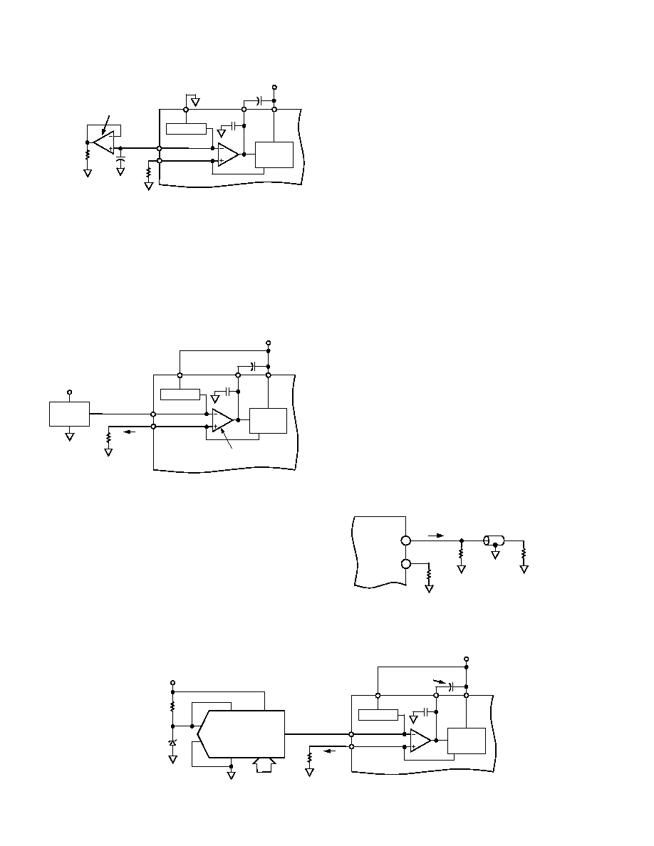
Figure 13. Internal Reference Configuration
The internal reference can be disabled by connecting REFLO to
AVDD. In this case, an external reference may then be applied
to REFIO as shown in Figure 14. The external reference may
provide either a fixed reference voltage to enhance accuracy and
drift performance or a varying reference voltage for gain control.
Note that the 0.1
F compensation capacitor is not required
since the internal reference is disabled, and the high input
impedance (i.e., 1 M
) of REFIO minimizes any loading of the
external reference.
50pF
COMP1
+1.2V REF
AVDD
REFLO
CURRENT
SOURCE
ARRAY
0.1 F
AVDD
REFIO
FS ADJ
RSET
AD9708
EXTERNAL
REF
IREF =
VREFIO/RSET
AVDD
REFERENCE
CONTROL
AMPLIFIER
VREFIO
Figure 14. External Reference Configuration
The AD9708 also contains an internal control amplifier that is
used to regulate the DAC’s full-scale output current, IOUTFS.
The control amplifier is configured as a V-I converter, as shown
in Figure 14, such that its current output, IREF, is determined by
the ratio of the VREFIO and an external resistor, RSET, as stated
in Equation 4. The control amplifier allows a wide (10:1)
adjustment span of IOUTFS over a 2 mA to 20 mA range by setting
IREF between 62.5
A and 625 A. The wide adjustment span of
IOUTFS provides several application benefits. The first benefit
relates directly to the power dissipation of the AD9708, which is
proportional to IOUTFS (refer to the POWER DISSIPATION
section). The second benefit relates to the 20 dB adjustment,
which is useful for system gain control purposes.
The small signal bandwidth of the reference control amplifier is
approximately 1.8 MHz and can be reduced by connecting an
external capacitor between COMP1 and AVDD. The output of
the control amplifier, COMP1, is internally compensated via a
50 pF capacitor that limits the control amplifier small-signal
bandwidth and reduces its output impedance. Any additional
external capacitance further limits the bandwidth and acts as
a filter to reduce the noise contribution from the reference
amplifier. If IREF is fixed for an application, a 0.1
F ceramic chip
capacitor is recommended.
IREF can be varied for a fixed RSET by disabling the internal
reference and varying the common-mode voltage over its
compliance range of 1.25 V to 0.10 V. REFIO can be driven by
a single-supply amplifier or DAC, thus allowing IREF to be var-
ied for a fixed RSET. Since the input impedance of REFIO is
approximately 1 M
, a simple R-2R ladder DAC configured in
the voltage mode topology may be used to control the gain. This
circuit is shown in Figure 15 using the AD7524 and an external
1.2 V reference, the AD1580. Note another AD9708 could also
be used as the gain control DAC since it can also provide a
programmable unipolar output up to 1.2 V.
ANALOG OUTPUTS AND OUTPUT CONFIGURATIONS
The AD9708 produces two complementary current outputs,
IOUTA and IOUTB, which may be converted into complementary
single-ended voltage outputs, VOUTA and VOUTB, via a load resistor,
RLOAD, as described in the DAC TRANSFER FUNCTION
section. Figure 16 shows the AD9708 configured to provide a
positive unipolar output range of approximately 0 V to +0.5 V
for a double terminated 50
cable for a nominal full-scale
current, IOUTFS, of 20 mA. In this case, RLOAD represents the
equivalent load resistance seen by IOUTA or IOUTB and is
equal to 25
. The unused output (IOUTA or IOUTB) can be
connected to ACOM directly or via a matching RLOAD. Different
values of IOUTFS and RLOAD can be selected as long as the posi-
tive compliance range is adhered to.
AD9708
IOUTA
IOUTB 21
50
25
50
VOUTA = 0 TO +0.5V
IOUTFS = 20mA
22
Figure 16. 0 V to +0.5 V Unbuffered Voltage Output
Alternatively, an amplifier could be configured as an I-V converter
thus converting IOUTA or IOUTB into a negative unipolar
1.2V
50pF
COMP1
+1.2V REF
AVDD
REFLO
CURRENT
SOURCE
ARRAY
AVDD
REFIO
FS ADJ
RSET
AD9708
IREF =
VREF/RSET
AVDD
OPTIONAL
BANDLIMITING
CAPACITOR
VREF
VDD
RFB
OUT1
OUT2
AGND
DB7–DB0
AD7524
AD1580
0.1V TO 1.2V
Figure 15. Single-Supply Gain Control Circuit
相关PDF资料 |
PDF描述 |
|---|---|
| MPC9456ACR2 | IC CLK BUFF DVDR MUX 1:10 32LQFP |
| AD5444YRM-REEL7 | IC DAC 12BIT MULTIPLYING 10-MSOP |
| AD5647RBRMZ-REEL7 | IC DAC NANO 14BIT DUAL 10-MSOP |
| LTC1426CS8#TR | IC DAC PWM 6BIT DUAL MCPWR 8SOIC |
| AD5341BRUZ-REEL7 | IC DAC 12BIT SNGL VOUT 20-TSSOP |
相关代理商/技术参数 |
参数描述 |
|---|---|
| AD9708ARZ | 功能描述:IC DAC 8BIT 100MSPS 28-SOIC RoHS:是 类别:集成电路 (IC) >> 数据采集 - 数模转换器 系列:TxDAC® 产品培训模块:Lead (SnPb) Finish for COTS Obsolescence Mitigation Program 标准包装:50 系列:- 设置时间:4µs 位数:12 数据接口:串行 转换器数目:2 电压电源:单电源 功率耗散(最大):- 工作温度:-40°C ~ 85°C 安装类型:表面贴装 封装/外壳:8-TSSOP,8-MSOP(0.118",3.00mm 宽) 供应商设备封装:8-uMAX 包装:管件 输出数目和类型:2 电压,单极 采样率(每秒):* 产品目录页面:1398 (CN2011-ZH PDF) |
| AD9708ARZ | 制造商:Analog Devices 功能描述:IC 8BIT DAC 100MSPS 28SOIC 制造商:Analog Devices 功能描述:IC, 8BIT DAC, 100MSPS, 28SOIC |
| AD9708ARZRL | 功能描述:IC DAC 8BIT 100MSPS 28-SOIC RoHS:是 类别:集成电路 (IC) >> 数据采集 - 数模转换器 系列:TxDAC® 产品培训模块:LTC263x 12-, 10-, and 8-Bit VOUT DAC Family 特色产品:LTC2636 - Octal 12-/10-/8-Bit SPI VOUT DACs with 10ppm/°C Reference 标准包装:91 系列:- 设置时间:4µs 位数:10 数据接口:MICROWIRE?,串行,SPI? 转换器数目:8 电压电源:单电源 功率耗散(最大):2.7mW 工作温度:-40°C ~ 85°C 安装类型:表面贴装 封装/外壳:14-WFDFN 裸露焊盘 供应商设备封装:14-DFN-EP(4x3) 包装:管件 输出数目和类型:8 电压,单极 采样率(每秒):* |
| AD9708-EB | 制造商:Analog Devices 功能描述:Evaluation Board For AD9708 |
| AD9708-EBZ | 功能描述:BOARD EVAL FOR AD9708 RoHS:是 类别:编程器,开发系统 >> 评估板 - 数模转换器 (DAC) 系列:TxDAC® 产品培训模块:Lead (SnPb) Finish for COTS Obsolescence Mitigation Program 标准包装:1 系列:- DAC 的数量:4 位数:12 采样率(每秒):- 数据接口:串行,SPI? 设置时间:3µs DAC 型:电流/电压 工作温度:-40°C ~ 85°C 已供物品:板 已用 IC / 零件:MAX5581 |
发布紧急采购,3分钟左右您将得到回复。