参数资料
| 型号: | AD9708ARZRL |
| 厂商: | Analog Devices Inc |
| 文件页数: | 11/16页 |
| 文件大小: | 0K |
| 描述: | IC DAC 8BIT 100MSPS 28-SOIC |
| 产品培训模块: | Data Converter Fundamentals DAC Architectures |
| 标准包装: | 1,000 |
| 系列: | TxDAC® |
| 设置时间: | 35ns |
| 位数: | 8 |
| 数据接口: | 并联 |
| 转换器数目: | 1 |
| 电压电源: | 模拟和数字 |
| 功率耗散(最大): | 175mW |
| 工作温度: | -40°C ~ 85°C |
| 安装类型: | 表面贴装 |
| 封装/外壳: | 28-SOIC(0.295",7.50mm 宽) |
| 供应商设备封装: | 28-SOIC W |
| 包装: | 带卷 (TR) |
| 输出数目和类型: | 2 电流,单极;2 电流,双极 |
| 采样率(每秒): | 125M |
| 配用: | AD9708-EBZ-ND - BOARD EVAL FOR AD9708 |
AD9708
–4–
REV. B
ABSOLUTE MAXIMUM RATINGS*
With
Parameter
Respect to
Min
Max
Units
AVDD
ACOM
–0.3
+6.5
V
DVDD
DCOM
–0.3
+6.5
V
ACOM
DCOM
–0.3
+0.3
V
AVDD
DVDD
–6.5
+6.5
V
CLOCK, SLEEP
DCOM
–0.3
DVDD + 0.3
V
Digital Inputs
DCOM
–0.3
DVDD + 0.3
V
IOUTA, IOUTB
ACOM
–1.0
AVDD + 0.3
V
COMP1, COMP2
ACOM
–0.3
AVDD + 0.3
V
REFIO, FSADJ
ACOM
–0.3
AVDD + 0.3
V
REFLO
ACOM
–0.3
+0.3
V
Junction Temperature
+150
°C
Storage Temperature
–65
+150
°C
Lead Temperature
(10 sec)
+300
°C
*Stresses above those listed under Absolute Maximum Ratings may cause perma-
nent damage to the device. This is a stress rating only; functional operation of the
device at these or any other conditions above those indicated in the operational
sections of this specification is not implied. Exposure to absolute maximum
ratings for extended periods may effect device reliability.
THERMAL CHARACTERISTICS
Thermal Resistance
28-Lead 300 mil SOIC
θ
JA = 71.4
°C/W
θ
JC = 23
°C/W
28-Lead TSSOP
θ
JA = 97.9
°C/W
θ
JC = 14.0
°C/W
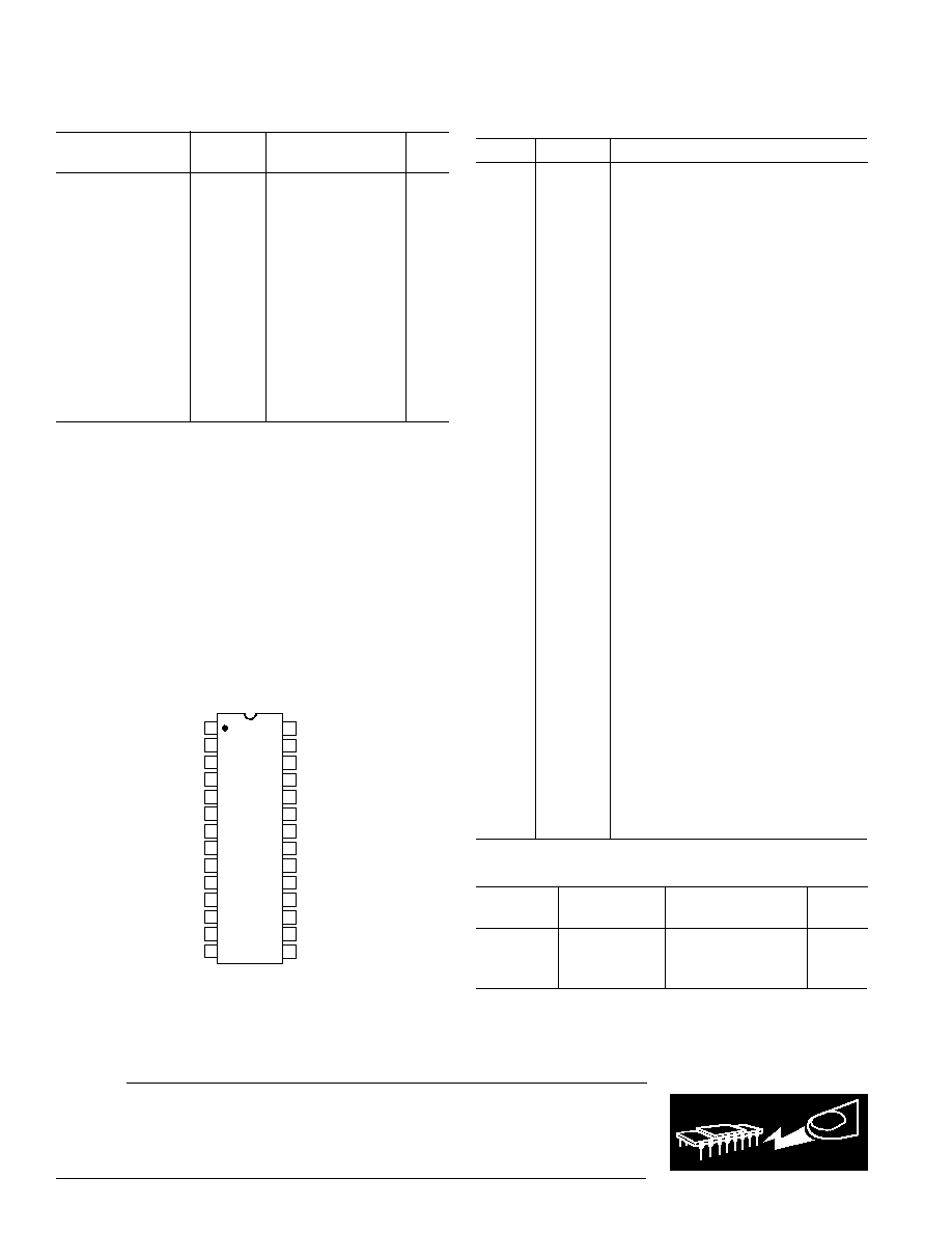
PIN CONFIGURATION
14
13
12
11
17
16
15
20
19
18
10
9
8
1
2
3
4
7
6
5
TOP VIEW
(Not to Scale)
28
27
26
25
24
23
22
21
AD9708
NC = NO CONNECT
(MSB) DB7
DB6
DB5
DB4
DB3
DB2
DB1
DB0
NC
CLOCK
DVDD
DCOM
NC
AVDD
COMP2
IOUTA
IOUTB
ACOM
COMP1
FS ADJ
REFIO
REFLO
SLEEP
CAUTION
ESD (electrostatic discharge) sensitive device. Electrostatic charges as high as 4000 V readily
accumulate on the human body and test equipment and can discharge without detection.
Although the AD9708 features proprietary ESD protection circuitry, permanent damage may
occur on devices subjected to high energy electrostatic discharges. Therefore, proper ESD
precautions are recommended to avoid performance degradation or loss of functionality.
PIN FUNCTION DESCRIPTIONS
Pin No.
Name
Description
1
DB7
Most Significant Data Bit (MSB).
2–7
DB6–DB1
Data Bits 1–6.
8
DB0
Least Significant Data Bit (LSB).
9–14, 25 NC
No Internal Connection.
15
SLEEP
Power-Down Control Input. Active
High. Contains active pull-down circuit,
thus may be left unterminated if not
used.
16
REFLO
Reference Ground when Internal 1.2 V
Reference Used. Connect to AVDD to
disable internal reference.
17
REFIO
Reference Input/Output. Serves as
reference input when internal reference
disabled (i.e., Tie REFLO to AVDD).
Serves as 1.2 V reference output when
internal reference activated (i.e., Tie
REFLO to ACOM). Requires 0.1
F
capacitor to ACOM when internal
reference activated.
18
FS ADJ
Full-Scale Current Output Adjust.
19
COMP1
Bandwidth/Noise Reduction Node.
Add 0.1
F to AVDD for optimum
performance.
20
ACOM
Analog Common.
21
IOUTB
Complementary DAC Current Output.
Full-scale current when all data bits
are 0s.
22
IOUTA
DAC Current Output. Full-scale
current when all data bits are 1s.
23
COMP2
Internal Bias Node for Switch Driver
Circuitry. Decouple to ACOM with
0.1
F capacitor.
24
AVDD
Analog Supply Voltage (+2.7 V to
+5.5 V).
26
DCOM
Digital Common.
27
DVDD
Digital Supply Voltage (+2.7 V to
+5.5 V).
28
CLOCK
Clock Input. Data latched on positive
edge of clock.
ORDERING GUIDE
Temperature
Package
Model
Range
Descriptions
Options*
AD9708AR
–40
°C to +85°C 28-Lead 300 Mil SOIC R-28
AD9708ARU –40
°C to +85°C 28-Lead TSSOP
RU-28
AD9708-EB
Evaluation Board
*R = Small Outline IC; RU = Thin Small Outline IC.
WARNING!
ESD SENSITIVE DEVICE
相关PDF资料 |
PDF描述 |
|---|---|
| VI-JNH-MY | CONVERTER MOD DC/DC 52V 50W |
| V110A15H400BL | CONVERTER MOD DC/DC 15V 400W |
| VE-BNB-MV-F3 | CONVERTER MOD DC/DC 95V 150W |
| VE-BN1-MV-F2 | CONVERTER MOD DC/DC 12V 150W |
| V110A15H400B3 | CONVERTER MOD DC/DC 15V 400W |
相关代理商/技术参数 |
参数描述 |
|---|---|
| AD9708-EB | 制造商:Analog Devices 功能描述:Evaluation Board For AD9708 |
| AD9708-EBZ | 功能描述:BOARD EVAL FOR AD9708 RoHS:是 类别:编程器,开发系统 >> 评估板 - 数模转换器 (DAC) 系列:TxDAC® 产品培训模块:Lead (SnPb) Finish for COTS Obsolescence Mitigation Program 标准包装:1 系列:- DAC 的数量:4 位数:12 采样率(每秒):- 数据接口:串行,SPI? 设置时间:3µs DAC 型:电流/电压 工作温度:-40°C ~ 85°C 已供物品:板 已用 IC / 零件:MAX5581 |
| AD9709 | 制造商:AD 制造商全称:Analog Devices 功能描述:Analog Devices: Data Converters: DAC 8-Bit, 10 ns to 100 ns Converters Selection Table |
| AD9709_09 | 制造商:AD 制造商全称:Analog Devices 功能描述:8-Bit, 125 MSPS, Dual TxDAC Digital-to-Analog Converter |
| AD9709ASF | 制造商:Analog Devices 功能描述:8BIT DUAL DAC W/POLY FUSE CALIBRATION - Bulk |
发布紧急采购,3分钟左右您将得到回复。