参数资料
| 型号: | AD9708ARZRL |
| 厂商: | Analog Devices Inc |
| 文件页数: | 2/16页 |
| 文件大小: | 0K |
| 描述: | IC DAC 8BIT 100MSPS 28-SOIC |
| 产品培训模块: | Data Converter Fundamentals DAC Architectures |
| 标准包装: | 1,000 |
| 系列: | TxDAC® |
| 设置时间: | 35ns |
| 位数: | 8 |
| 数据接口: | 并联 |
| 转换器数目: | 1 |
| 电压电源: | 模拟和数字 |
| 功率耗散(最大): | 175mW |
| 工作温度: | -40°C ~ 85°C |
| 安装类型: | 表面贴装 |
| 封装/外壳: | 28-SOIC(0.295",7.50mm 宽) |
| 供应商设备封装: | 28-SOIC W |
| 包装: | 带卷 (TR) |
| 输出数目和类型: | 2 电流,单极;2 电流,双极 |
| 采样率(每秒): | 125M |
| 配用: | AD9708-EBZ-ND - BOARD EVAL FOR AD9708 |
AD9708
–10–
REV. B
POWER DISSIPATION
The power dissipation, PD, of the AD9708 is dependent on
several factors, including: (1) AVDD and DVDD, the power
supply voltages; (2) IOUTFS, the full-scale current output; (3)
fCLOCK, the update rate; (4) and the reconstructed digital input
waveform. The power dissipation is directly proportional to the
analog supply current, IAVDD, and the digital supply current,
IDVDD. IAVDD is directly proportional to IOUTFS, as shown in
Figure 19, and is insensitive to fCLOCK.
Conversely, IDVDD is dependent on both the digital input wave-
form, fCLOCK, and digital supply DVDD. Figures 20 and 21
show IDVDD as a function of full-scale sine wave output ratios
(fOUT/fCLOCK) for various update rates with DVDD = 5 V and
DVDD = 3 V, respectively. Note, how IDVDD is reduced by more
than a factor of 2 when DVDD is reduced from 5 V to 3 V.
APPLYING THE AD9708
Power and Grounding Considerations
In systems seeking to simultaneously achieve high speed and
high performance, the implementation and construction of the
printed circuit board design is often as important as the circuit
design. Proper RF techniques must be used in device selection
placement and routing and supply bypassing and grounding.
The evaluation board for the AD9708, which uses a four layer
PC board, serves as a good example for the above mentioned
considerations. The evaluation board provides an illustration of
the recommended printed circuit board ground, power and
signal plane layouts.
Proper grounding and decoupling should be a primary objective
in any high speed system. The AD9708 features separate analog
and digital supply and ground pins to optimize the management
of analog and digital ground currents in a system. In general,
AVDD, the analog supply, should be decoupled to ACOM, the
analog common, as close to the chip as physically possible. Simi-
larly, DVDD, the digital supply, should be decoupled to DCOM
as close as physically as possible.
For those applications requiring a single +5 V or +3 V supply
for both the analog and digital supply, a clean analog supply
may be generated using the circuit shown in Figure 22. The
circuit consists of a differential LC filter with separate power
supply and return lines. Lower noise can be attained using low
ESR type electrolytic and tantalum capacitors.
IOUTFS – mA
30
0
220
46
8
10
12
14
16
18
25
20
15
10
5
I AVDD
–
mA
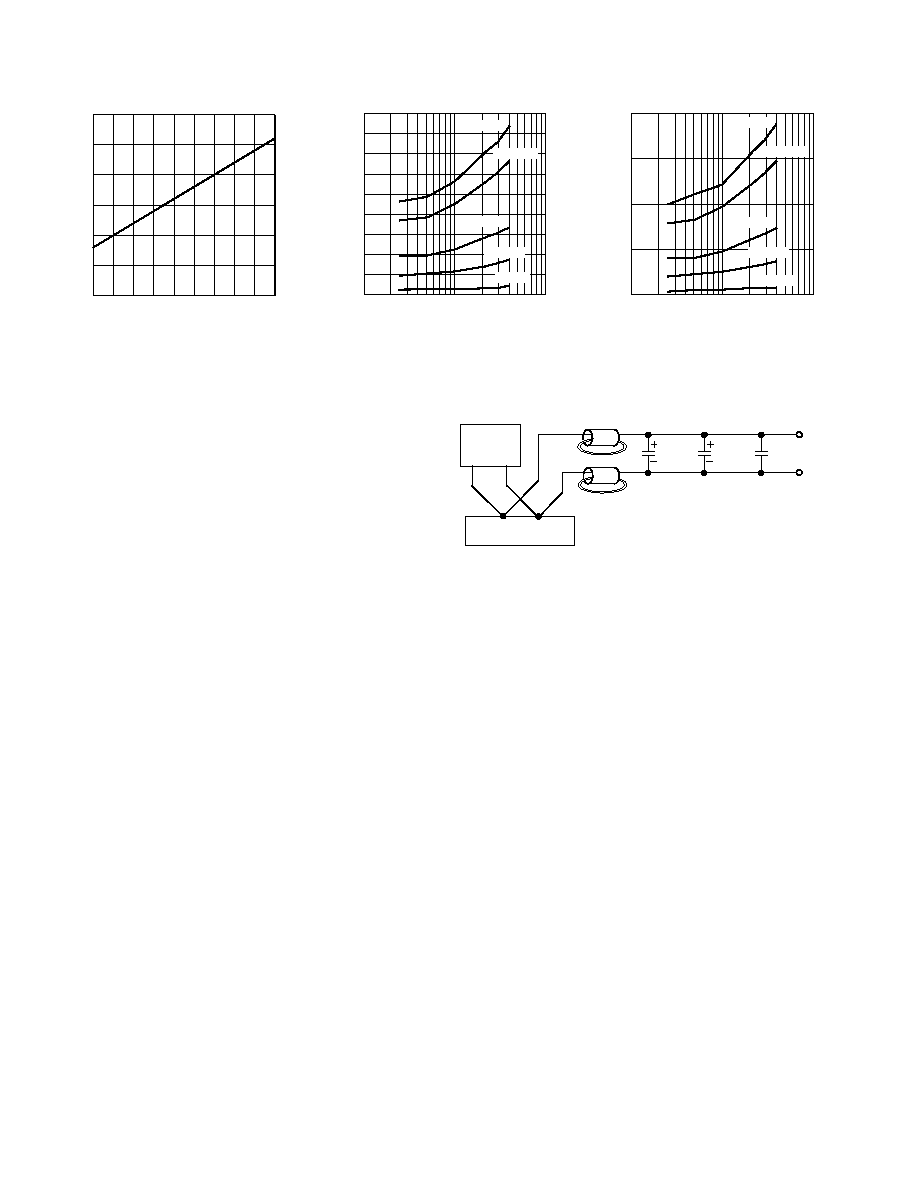
Figure 19. IAVDD vs. IOUTFS
RATIO (fOUT/fCLK)
18
16
0
0.01
1
0.1
I DVDD
–
mA
8
6
4
2
12
10
14
5MSPS
25MSPS
50MSPS
100MSPS
125MSPS
Figure 20. IDVDD vs. Ratio
@ DVDD = 5 V
100 F
ELECT.
10-22 F
TANT.
0.1 F
CER.
TTL/CMOS
LOGIC
CIRCUITS
+5V OR +3V
POWER SUPPLY
FERRITE
BEADS
AVDD
ACOM
Figure 22. Differential LC Filter for Single +5 V or +3 V
Applications
Maintaining low noise on power supplies and ground is critical
to obtaining optimum results from the AD9708. If properly
implemented, ground planes can perform a host of functions on
high speed circuit boards: bypassing, shielding, current trans-
port, etc. In mixed signal design, the analog and digital portions
of the board should be distinct from each other, with the analog
ground plane confined to the areas covering the analog signal
traces, and the digital ground plane confined to areas covering
the digital interconnects.
All analog ground pins of the DAC, reference and other analog
components, should be tied directly to the analog ground plane.
The two ground planes should be connected by a path 1/8 to
1/4 inch wide underneath or within 1/2 inch of the DAC to
maintain optimum performance. Care should be taken to ensure
that the ground plane is uninterrupted over crucial signal paths.
On the digital side, this includes the digital input lines running
to the DAC as well as any clock signals. On the analog side, this
includes the DAC output signal, reference signal and the supply
feeders.
The use of wide runs or planes in the routing of power lines is
also recommended. This serves the dual role of providing a low
series impedance power supply to the part, as well as providing
some “free” capacitive decoupling to the appropriate ground
plane. It is essential that care be taken in the layout of signal and
power ground interconnects to avoid inducing extraneous
voltage drops in the signal ground paths. It is recommended that
all connections be short, direct and as physically close to the
package as possible in order to minimize the sharing of conduc-
tion paths between different currents. When runs exceed an inch
in length, strip line techniques with proper termination resistor
RATIO (fOUT/fCLK)
8
0
0.01
1
0.1
I DVDD
–
mA
6
4
2
5MSPS
25MSPS
50MSPS
100MSPS
125MSPS
Figure 21. IDVDD vs. Ratio
@ DVDD = 3 V
相关PDF资料 |
PDF描述 |
|---|---|
| VI-JNH-MY | CONVERTER MOD DC/DC 52V 50W |
| V110A15H400BL | CONVERTER MOD DC/DC 15V 400W |
| VE-BNB-MV-F3 | CONVERTER MOD DC/DC 95V 150W |
| VE-BN1-MV-F2 | CONVERTER MOD DC/DC 12V 150W |
| V110A15H400B3 | CONVERTER MOD DC/DC 15V 400W |
相关代理商/技术参数 |
参数描述 |
|---|---|
| AD9708-EB | 制造商:Analog Devices 功能描述:Evaluation Board For AD9708 |
| AD9708-EBZ | 功能描述:BOARD EVAL FOR AD9708 RoHS:是 类别:编程器,开发系统 >> 评估板 - 数模转换器 (DAC) 系列:TxDAC® 产品培训模块:Lead (SnPb) Finish for COTS Obsolescence Mitigation Program 标准包装:1 系列:- DAC 的数量:4 位数:12 采样率(每秒):- 数据接口:串行,SPI? 设置时间:3µs DAC 型:电流/电压 工作温度:-40°C ~ 85°C 已供物品:板 已用 IC / 零件:MAX5581 |
| AD9709 | 制造商:AD 制造商全称:Analog Devices 功能描述:Analog Devices: Data Converters: DAC 8-Bit, 10 ns to 100 ns Converters Selection Table |
| AD9709_09 | 制造商:AD 制造商全称:Analog Devices 功能描述:8-Bit, 125 MSPS, Dual TxDAC Digital-to-Analog Converter |
| AD9709ASF | 制造商:Analog Devices 功能描述:8BIT DUAL DAC W/POLY FUSE CALIBRATION - Bulk |
发布紧急采购,3分钟左右您将得到回复。