参数资料
| 型号: | AD9734BBCZRL |
| 厂商: | Analog Devices Inc |
| 文件页数: | 47/72页 |
| 文件大小: | 0K |
| 描述: | IC DAC 10BIT 1.2GSPS 160-CSPBGA |
| 产品培训模块: | Data Converter Fundamentals DAC Architectures |
| 标准包装: | 1,500 |
| 位数: | 10 |
| 数据接口: | 并联 |
| 转换器数目: | 1 |
| 电压电源: | 模拟和数字 |
| 功率耗散(最大): | 550mW |
| 工作温度: | -40°C ~ 85°C |
| 安装类型: | 表面贴装 |
| 封装/外壳: | 160-LFBGA,CSPBGA |
| 供应商设备封装: | 160-CSPBGA(12x12) |
| 包装: | 带卷 (TR) |
| 输出数目和类型: | 2 电流,单极 |
| 采样率(每秒): | 1.2G |
第1页第2页第3页第4页第5页第6页第7页第8页第9页第10页第11页第12页第13页第14页第15页第16页第17页第18页第19页第20页第21页第22页第23页第24页第25页第26页第27页第28页第29页第30页第31页第32页第33页第34页第35页第36页第37页第38页第39页第40页第41页第42页第43页第44页第45页第46页当前第47页第48页第49页第50页第51页第52页第53页第54页第55页第56页第57页第58页第59页第60页第61页第62页第63页第64页第65页第66页第67页第68页第69页第70页第71页第72页
AD9734/AD9735/AD9736
Rev. A | Page 51 of 72
DAC OUTPUT DISTORTION SOURCES
The second harmonic is mostly due to an imbalance in the
output load. The dc transfer characteristic of the DAC is capable
of second harmonic distortion of at least 75 dBc. Output load
imbalance or digital data noise coupling onto DACCLK causes
additional second harmonic distortion.
The DAC architecture inherently generates third harmonics, the
levels of which depend on the output frequency and amplitude
generated. If any output signal is rectified and coupled back
onto the DAC clock, it can generate additional third-harmonic
energy.
The distortion components should be identical in amplitude
and phase at both AD973x outputs. Even though each single-
ended output includes a large amount of second-harmonic
energy, a careful differential-to-single-ended conversion can
remove most of it. Optimum performance at high intermediate
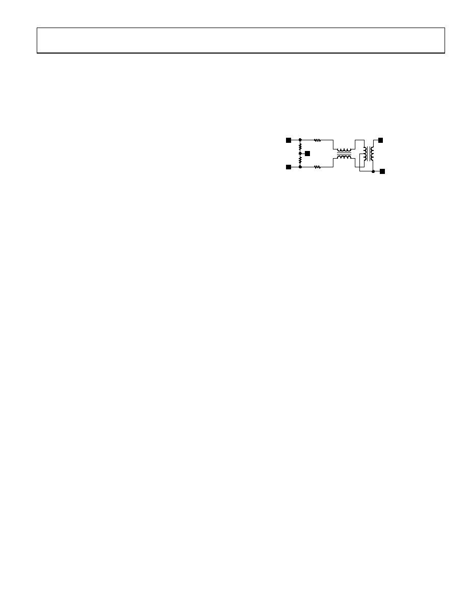
frequency (IF) output is obtained with the output circuit shown
in Figure 93.
This is the configuration implemented on the evaluation board
(Figure 107). The 20 Ω series resistors allow the DAC to drive a
less reactive load, which improves distortion. Further improvement
is realized by adding the Balun T3 to help provide an equal load
to both DAC outputs.
04862-091
IOUTA
IOUTB
J2, 50
Ω OUTPUT
AVSS
R17
20
Ω
15
6
5
1
34
4
3
R19
20
Ω
T3
T1
AVSS
R8
50
Ω
R6
50
Ω
Figure 93. IF Signal Output Circuit
Because T1 has a differential input, but a single-ended output,
Pin 4 of T1 has a higher capacitance to ground due to parasitics
to Pin 3. T1 Pin 6 has lower parasitic capacitance to ground
because it drives 50 Ω at Pin 1. This presents an unbalanced
load to the DAC output, so T3 is added to improve the load
balancing. Refer to Figure 107 for the transformer part numbers.
相关PDF资料 |
PDF描述 |
|---|---|
| VI-B3P-MY-B1 | CONVERTER MOD DC/DC 13.8V 50W |
| VI-230-MW-B1 | CONVERTER MOD DC/DC 5V 100W |
| VI-B3N-MY-B1 | CONVERTER MOD DC/DC 18.5V 50W |
| LTC1599BCG#TRPBF | IC D/A CONV 16BIT MLTPLYNG24SSOP |
| VI-B3M-MY-B1 | CONVERTER MOD DC/DC 10V 50W |
相关代理商/技术参数 |
参数描述 |
|---|---|
| AD9734BBCZRL1 | 制造商:AD 制造商全称:Analog Devices 功能描述:10-/12-/14-Bit, 1200 MSPS DACS |
| AD9734-DPG2-EBZ | 功能描述:BOARD EVAL FOR AD9734 RoHS:是 类别:编程器,开发系统 >> 评估板 - 数模转换器 (DAC) 系列:- 产品培训模块:Lead (SnPb) Finish for COTS Obsolescence Mitigation Program 标准包装:1 系列:- DAC 的数量:4 位数:12 采样率(每秒):- 数据接口:串行,SPI? 设置时间:3µs DAC 型:电流/电压 工作温度:-40°C ~ 85°C 已供物品:板 已用 IC / 零件:MAX5581 |
| AD9734-EB | 制造商:Analog Devices 功能描述:EVAL BD FOR AD9735 DAC, 10-/12-/14BIT, 1200 MSPS DACS - Trays |
| AD9734-EBZ | 制造商:Analog Devices 功能描述:EVAL BD FOR AD9735 DAC, 10-/12-/14BIT, 1200 MSPS DACS - Bulk |
| AD9735 | 制造商:AD 制造商全称:Analog Devices 功能描述:14/12/10-Bit, 1200 MSPS D/A Converters |
发布紧急采购,3分钟左右您将得到回复。