参数资料
| 型号: | AD9740ACPZ |
| 厂商: | Analog Devices Inc |
| 文件页数: | 8/32页 |
| 文件大小: | 0K |
| 描述: | IC DAC 10BIT 210MSPS 32-LFCSP |
| 产品培训模块: | Data Converter Fundamentals DAC Architectures |
| 标准包装: | 1 |
| 系列: | TxDAC® |
| 设置时间: | 11ns |
| 位数: | 10 |
| 数据接口: | 并联 |
| 转换器数目: | 1 |
| 电压电源: | 模拟和数字 |
| 功率耗散(最大): | 145mW |
| 工作温度: | -40°C ~ 85°C |
| 安装类型: | 表面贴装 |
| 封装/外壳: | 32-VFQFN 裸露焊盘,CSP |
| 供应商设备封装: | 32-LFCSP-VQ(5x5) |
| 包装: | 托盘 |
| 输出数目和类型: | 2 电流,单极;2 电流,双极 |
| 采样率(每秒): | 210M |
| 产品目录页面: | 785 (CN2011-ZH PDF) |
| 配用: | AD9740ACP-PCBZ-ND - BOARD EVAL FOR AD9740ACP |
第1页第2页第3页第4页第5页第6页第7页当前第8页第9页第10页第11页第12页第13页第14页第15页第16页第17页第18页第19页第20页第21页第22页第23页第24页第25页第26页第27页第28页第29页第30页第31页第32页
AD9740
Rev. B | Page 16 of 32
In the differential input mode, the clock input functions as a
high impedance differential pair. The common-mode level of
the CLK+ and CLK inputs can vary from 0.75 V to 2.25 V, and
the differential voltage can be as low as 0.5 V p-p. This mode
can be used to drive the clock with a differential sine wave
because the high gain bandwidth of the differential inputs
converts the sine wave into a single-ended square wave internally.
The final clock mode allows for a reduced external component
count when the DAC clock is distributed on the board using
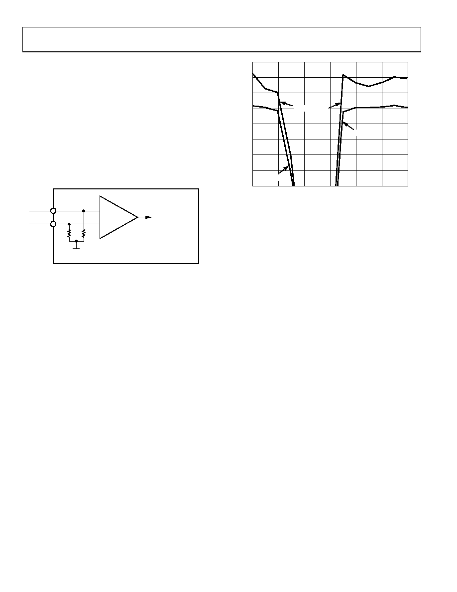
PECL logic. The internal termination configuration is shown in
Figure 27. These termination resistors are untrimmed and can
vary up to ±20%. However, matching between the resistors
should generally be better than ±1%.
CLK+
TO DAC CORE
CLK–
VTT = 1.3V NOM
50
Ω
50
Ω
AD9740
CLOCK
RECEIVER
02911-
025
Figure 27. Clock Termination in PECL Mode
DAC TIMING
Input Clock and Data Timing Relationship
Dynamic performance in a DAC is dependent on the
relationship between the position of the clock edges and the
time at which the input data changes. The AD9740 is rising
edge triggered, and so exhibits dynamic performance sensitivity
when the data transition is close to this edge. In general, the
goal when applying the AD9740 is to make the data transition
close to the falling clock edge. This becomes more important as
the sample rate increases. Figure 28 shows the relationship of
SFDR to clock placement with different sample rates. Note that
at the lower sample rates, more tolerance is allowed in clock
placement, while at higher rates, more care must be taken.
–3
–2
2
–1
0
1
65
75
ns
dB
3
55
45
35
60
70
50
40
50MHz SFDR
20MHz SFDR
50MHz SFDR
02911-026
Figure 28. SFDR vs. Clock Placement @
fOUT = 20 MHz and 50 MHz (fCLOCK = 165 MSPS)
Sleep Mode Operation
The AD9740 has a power-down function that turns off the output
current and reduces the supply current to less than 6 mA over the
specified supply range of 2.7 V to 3.6 V and the temperature range.
This mode can be activated by applying a Logic Level 1 to the
SLEEP pin. The SLEEP pin logic threshold is equal to 0.5 Ω
AVDD. This digital input also contains an active pull-down
circuit that ensures that the AD9740 remains enabled if this
input is left disconnected. The AD9740 takes less than 50 ns
to power down and approximately 5 μs to power back up.
POWER DISSIPATION
The power dissipation, PD, of the AD9740 is dependent on
several factors that include:
The power supply voltages (AVDD, CLKVDD, and
DVDD)
The full-scale current output (IOUTFS)
The update rate (fCLOCK)
The reconstructed digital input waveform
The power dissipation is directly proportional to the analog
supply current, IAVDD, and the digital supply current, IDVDD. IAVDD
insensitive to fCLOCK. Conversely, IDVDD is dependent on both the
shows IDVDD as a function of full-scale sine wave output ratios
(fOUT/fCLOCK) for various update rates with DVDD = 3.3 V.
相关PDF资料 |
PDF描述 |
|---|---|
| VI-J4R-MZ-F4 | CONVERTER MOD DC/DC 7.5V 25W |
| VI-J4R-MZ-F3 | CONVERTER MOD DC/DC 7.5V 25W |
| VI-J4L-MZ-F1 | CONVERTER MOD DC/DC 28V 25W |
| AD5308BRUZ | IC DAC 8BIT OCTAL W/BUFF 16TSSOP |
| SI5322-C-GM | IC PREC CLOCK MULTIPLIER 36-QFN |
相关代理商/技术参数 |
参数描述 |
|---|---|
| AD9740ACPZ1 | 制造商:AD 制造商全称:Analog Devices 功能描述:10-Bit, 210 MSPS TxDAC D/A Converter |
| AD9740ACPZRL7 | 功能描述:IC DAC 10BIT 210MSPS 32-LFCSP RoHS:是 类别:集成电路 (IC) >> 数据采集 - 数模转换器 系列:TxDAC® 产品培训模块:LTC263x 12-, 10-, and 8-Bit VOUT DAC Family 特色产品:LTC2636 - Octal 12-/10-/8-Bit SPI VOUT DACs with 10ppm/°C Reference 标准包装:91 系列:- 设置时间:4µs 位数:10 数据接口:MICROWIRE?,串行,SPI? 转换器数目:8 电压电源:单电源 功率耗散(最大):2.7mW 工作温度:-40°C ~ 85°C 安装类型:表面贴装 封装/外壳:14-WFDFN 裸露焊盘 供应商设备封装:14-DFN-EP(4x3) 包装:管件 输出数目和类型:8 电压,单极 采样率(每秒):* |
| AD9740AR | 制造商:Analog Devices 功能描述:DAC 1-CH Segment 10-bit 28-Pin SOIC W 制造商:Rochester Electronics LLC 功能描述:10 BIT 165 MSPS TXDAC D/A CONVERTER - Bulk 制造商:Analog Devices 功能描述:Digital-Analog Converter IC Interface Ty |
| AD9740ARRL | 制造商:Analog Devices 功能描述:DAC 1-CH Segment 10-bit 28-Pin SOIC W T/R 制造商:Analog Devices 功能描述:DAC SGL CURRENT STEERING 10-BIT 28SOIC W - Tape and Reel |
| AD9740ARU | 功能描述:IC DAC 10BIT 210MSPS 28-TSSOP RoHS:否 类别:集成电路 (IC) >> 数据采集 - 数模转换器 系列:TxDAC® 标准包装:47 系列:- 设置时间:2µs 位数:14 数据接口:并联 转换器数目:1 电压电源:单电源 功率耗散(最大):55µW 工作温度:-40°C ~ 85°C 安装类型:表面贴装 封装/外壳:28-SSOP(0.209",5.30mm 宽) 供应商设备封装:28-SSOP 包装:管件 输出数目和类型:1 电流,单极;1 电流,双极 采样率(每秒):* |
发布紧急采购,3分钟左右您将得到回复。