参数资料
| 型号: | AD9742ARUZRL7 |
| 厂商: | Analog Devices Inc |
| 文件页数: | 6/32页 |
| 文件大小: | 0K |
| 描述: | IC DAC 12BIT 210MSPS 28-TSSOP |
| 产品培训模块: | Data Converter Fundamentals DAC Architectures |
| 标准包装: | 1,000 |
| 系列: | TxDAC® |
| 设置时间: | 11ns |
| 位数: | 12 |
| 数据接口: | 并联 |
| 转换器数目: | 1 |
| 电压电源: | 模拟和数字 |
| 功率耗散(最大): | 145mW |
| 工作温度: | -40°C ~ 85°C |
| 安装类型: | 表面贴装 |
| 封装/外壳: | 28-TSSOP(0.173",4.40mm 宽) |
| 供应商设备封装: | 28-TSSOP |
| 包装: | 带卷 (TR) |
| 输出数目和类型: | 2 电流,单极;2 电流,双极 |
| 采样率(每秒): | 210M |
| 配用: | AD9742ACP-PCBZ-ND - BOARD EVAL FOR AD9742ACP |
第1页第2页第3页第4页第5页当前第6页第7页第8页第9页第10页第11页第12页第13页第14页第15页第16页第17页第18页第19页第20页第21页第22页第23页第24页第25页第26页第27页第28页第29页第30页第31页第32页
AD9742
Data Sheet
Rev. C | Page 14 of 32
The output impedance of IOUTA and IOUTB is determined by
the equivalent parallel combination of the PMOS switches
associated with the current sources and is typically 100 k in
parallel with 5 pF. It is also slightly dependent on the output
voltage (i.e., VOUTA and VOUTB) due to the nature of a PMOS
device. As a result, maintaining IOUTA and/or IOUTB at a
virtual ground via an I-V op amp configuration will result in
the optimum dc linearity. Note that the INL/DNL specifications
for the AD9742 are measured with IOUTA maintained at a
virtual ground via an op amp.
IOUTA and IOUTB also have a negative and positive voltage
compliance range that must be adhered to in order to achieve
optimum performance. The negative output compliance range
of 1 V is set by the breakdown limits of the CMOS process.
Operation beyond this maximum limit may result in a breakdown
of the output stage and affect the reliability of the AD9742.
The positive output compliance range is slightly dependent on
the full-scale output current, IOUTFS. It degrades slightly from its
nominal 1.2 V for an IOUTFS = 20 mA to 1 V for an IOUTFS = 2 mA.
The optimum distortion performance for a single-ended or
differential output is achieved when the maximum full-scale
signal at IOUTA and IOUTB does not exceed 0.5 V.
DIGITAL INPUTS
The AD9742 digital section consists of 12 input bit channels
and a clock input. The 12-bit parallel data inputs follow standard
positive binary coding, where DB11 is the most significant bit
(MSB) and DB0 is the least significant bit (LSB). IOUTA produces
a full-scale output current when all data bits are at Logic 1. IOUTB
produces a complementary output with the full-scale current
split between the two outputs as a function of the input code.
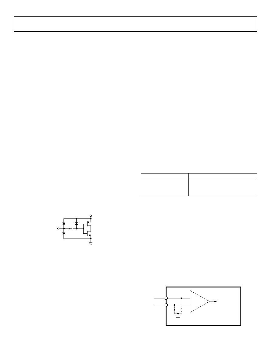
DVDD
DIGITAL
INPUT
02912-B-024
Figure 25. Equivalent Digital Input
The digital interface is implemented using an edge-triggered
master/slave latch. The DAC output updates on the rising edge
of the clock and is designed to support a clock rate as high as
210 MSPS. The clock can be operated at any duty cycle that meets
the specified latch pulse width. The setup and hold times can
also be varied within the clock cycle as long as the specified
minimum times are met, although the location of these
transition edges may affect digital feedthrough and distortion
performance. Best performance is typically achieved when the
input data transitions on the falling edge of a 50% duty cycle clock.
CLOCK INPUT
SOIC/TSSOP Packages
The 28-lead package options have a single-ended clock input
(CLOCK) that must be driven to rail-to-rail CMOS levels. The
quality of the DAC output is directly related to the clock quality,
and jitter is a key concern. Any noise or jitter in the clock will
translate directly into the DAC output. Optimal performance
will be achieved if the CLOCK input has a sharp rising edge,
since the DAC latches are positive edge triggered.
LFCSP Package
A configurable clock input is available in the LFCSP package,
which allows for one single-ended and two differential modes.
The mode selection is controlled by the CMODE input, as
summarized in Table 7. Connecting CMODE to CLKCOM
selects the single-ended clock input. In this mode, the CLK+
input is driven with rail-to-rail swings and the CLK input is
left floating. If CMODE is connected to CLKVDD, the differential
receiver mode is selected. In this mode, both inputs are high
impedance. The final mode is selected by floating CMODE. This
mode is also differential, but internal terminations for positive
emitter-coupled logic (PECL) are activated. There is no significant
performance difference between any of the three clock input modes.
Table 7. Clock Mode Selection
CMODE Pin
Clock Input Mode
CLKCOM
Single-Ended
CLKVDD
Differential
Float
PECL
The single-ended input mode operates in the same way as the
CLOCK input in the 28-lead packages, as described previously.
In the differential input mode, the clock input functions as a
high impedance differential pair. The common-mode level of
the CLK+ and CLK inputs can vary from 0.75 V to 2.25 V, and
the differential voltage can be as low as 0.5 V p-p. This mode
can be used to drive the clock with a differential sine wave since
the high gain bandwidth of the differential inputs will convert
the sine wave into a single-ended square wave internally.
The final clock mode allows for a reduced external component
count when the DAC clock is distributed on the board using
PECL logic. The internal termination configuration is shown in
Figure 26. These termination resistors are untrimmed and can
vary up to ±20%. However, matching between the resistors
should generally be better than ±1%.
CLK+
TO DAC CORE
CLK–
VTT = 1.3V NOM
50
50
AD9742
CLOCK
RECEIVER
02912-B-025
Figure 26. Clock Termination in PECL Mode\
相关PDF资料 |
PDF描述 |
|---|---|
| VI-B3Z-MU-B1 | CONVERTER MOD DC/DC 2V 80W |
| VI-B3Y-MU-B1 | CONVERTER MOD DC/DC 3.3V 132W |
| VI-J1F-MY | CONVERTER MOD DC/DC 72V 50W |
| VI-J1D-MY | CONVERTER MOD DC/DC 85V 50W |
| AD5060BRJZ-2REEL7 | IC DAC 16BIT SPI/SRL SOT23-8 |
相关代理商/技术参数 |
参数描述 |
|---|---|
| AD9742ARZ | 功能描述:IC DAC 12BIT 210MSPS 28-SOIC RoHS:是 类别:集成电路 (IC) >> 数据采集 - 数模转换器 系列:TxDAC® 标准包装:47 系列:- 设置时间:2µs 位数:14 数据接口:并联 转换器数目:1 电压电源:单电源 功率耗散(最大):55µW 工作温度:-40°C ~ 85°C 安装类型:表面贴装 封装/外壳:28-SSOP(0.209",5.30mm 宽) 供应商设备封装:28-SSOP 包装:管件 输出数目和类型:1 电流,单极;1 电流,双极 采样率(每秒):* |
| AD9742ARZRL | 功能描述:IC DAC 12BIT 210MSPS 28-SOIC RoHS:是 类别:集成电路 (IC) >> 数据采集 - 数模转换器 系列:TxDAC® 标准包装:47 系列:- 设置时间:2µs 位数:14 数据接口:并联 转换器数目:1 电压电源:单电源 功率耗散(最大):55µW 工作温度:-40°C ~ 85°C 安装类型:表面贴装 封装/外壳:28-SSOP(0.209",5.30mm 宽) 供应商设备封装:28-SSOP 包装:管件 输出数目和类型:1 电流,单极;1 电流,双极 采样率(每秒):* |
| AD9742-EB | 制造商:Analog Devices 功能描述:EVAL BOARDFOR AD9742 - Bulk |
| AD9742-EBZ | 制造商:AD 制造商全称:Analog Devices 功能描述:12-Bit, 210 MSPS TxDAC Digital-to-Analog Converter |
| AD9743 | 制造商:AD 制造商全称:Analog Devices 功能描述:Dual 8-/10-/12-/14-/16-Bit 250 MSPS Digital-to-Analog Converters |
发布紧急采购,3分钟左右您将得到回复。