- 您现在的位置:买卖IC网 > PDF目录17063 > AD9753-EB (Analog Devices Inc)BOARD EVAL FOR AD9753 PDF资料下载
参数资料
| 型号: | AD9753-EB |
| 厂商: | Analog Devices Inc |
| 文件页数: | 10/28页 |
| 文件大小: | 0K |
| 描述: | BOARD EVAL FOR AD9753 |
| 产品培训模块: | DAC Architectures |
| 标准包装: | 1 |
| 系列: | TxDAC+® |
| DAC 的数量: | 1 |
| 位数: | 12 |
| 采样率(每秒): | 300M |
| 数据接口: | 并联 |
| 设置时间: | 11ns |
| DAC 型: | 电流 |
| 工作温度: | -40°C ~ 85°C |
| 已供物品: | 板 |
| 已用 IC / 零件: | AD9753 |
| 相关产品: | AD9753ASTZRL-ND - IC DAC 12BIT 300MSPS 48LQFP AD9753ASTZ-ND - IC DAC 12BIT 300MSPS 48-LQFP |
第1页第2页第3页第4页第5页第6页第7页第8页第9页当前第10页第11页第12页第13页第14页第15页第16页第17页第18页第19页第20页第21页第22页第23页第24页第25页第26页第27页第28页
REV. B
–18–
AD9753
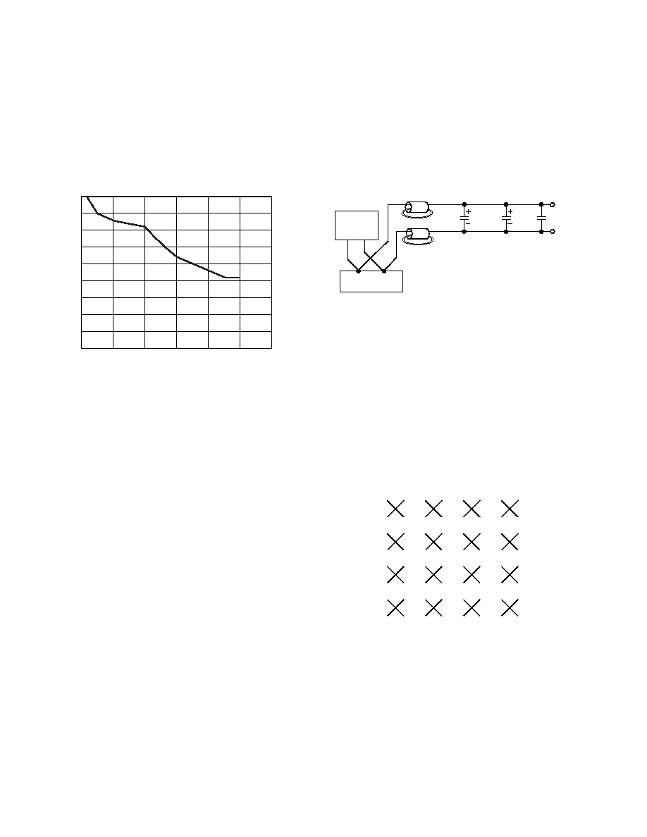
This is referred to as the Power Supply Rejection Ratio. For dc
variations of the power supply, the resulting performance of the
DAC directly corresponds to a gain error associated with the
DAC’s full-scale current, IOUTFS. AC noise on the dc supplies is
common in applications where the power distribution is gener-
ated by a switching power supply. Typically, switching power
supply noise will occur over the spectrum from tens of kHz to
several MHz. The PSRR versus the frequency of the AD9753
AVDD supply over this frequency range is shown in Figure 25.
FREQUENCY (MHz)
85
40
12
6
0
PSRR
(dB)
80
75
70
65
60
55
50
45
24
8
10
Figure 25. Power Supply Rejection Ratio
Note that the units in Figure 25 are given in units of (amps out/
volts in). Noise on the analog power supply has the effect of
modulating the internal switches, and therefore the output
current. The voltage noise on AVDD will thus be added in a
nonlinear manner to the desired IOUT. Due to the relative
different size of these switches, PSRR is very code-dependent.
This can produce a mixing effect that can modulate low fre-
quency power supply noise to higher frequencies. Worst-case
PSRR for either one of the differential DAC outputs will occur
when the full-scale current is directed toward that output. As a
result, the PSRR measurement in Figure 25 represents a worst-
case condition in which the digital inputs remain static and the
full-scale output current of 20 mA is directed to the DAC out-
put being measured.
An example serves to illustrate the effect of supply noise on the
analog supply. Suppose a switching regulator with a switching
frequency of 250 kHz produces 10 mV rms of noise and, for
simplicity sake (i.e., ignore harmonics), all of this noise is con-
centrated at 250 kHz. To calculate how much of this undesired
noise will appear as current noise superimposed on the DAC’s
full-scale current, IOUTFS, one must determine the PSRR in dB
using Figure 25 at 250 kHz. To calculate the PSRR for a given
RLOAD, such that the units of PSRR are converted from A/V to
V/V, adjust the curve in Figure 25 by the scaling factor 20
× Log
(RLOAD ). For instance, if RLOAD is 50
, the PSRR is reduced
by 34 dB, i.e., PSRR of the DAC at 250 kHz, which is 85 dB in
Figure 25, becomes 51 dB VOUT/VIN.
Proper grounding and decoupling should be a primary objective
in any high speed, high resolution system. The AD9753 features
separate analog and digital supply and ground pins to optimize
the management of analog and digital ground currents in a system.
In general, AVDD, the analog supply, should be decoupled to
ACOM, the analog common, as close to the chip as physically
possible. Similarly, DVDD, the digital supply, should be
decoupled to DCOM as close to the chip as physically possible.
For those applications that require a single 3.3 V supply for
both the analog and digital supplies, a clean analog supply may
be generated using the circuit shown in Figure 26. The circuit
consists of a differential LC filter with separate power supply
and return lines. Lower noise can be attained by using low ESR
type electrolytic and tantalum capacitors.
AVDD
ACOM
100 F
ELECT.
10 F
TANT.
0.1 F
CER.
TTL/CMOS
LOGIC
CIRCUITS
3.3V
POWER SUPPLY
FERRITE
BEADS
Figure 26. Differential LC Filter for a Single 3.3 V Application
APPLICATIONS
QAM/PSK Synthesis
Quadrature modulation (QAM or PSK) consists of two base-
band PAM (Pulse Amplitude Modulated) data channels. Both
channels are modulated by a common frequency carrier. How-
ever, the carriers for each channel are phase-shifted 90
° from
each other. This orthogonality allows twice the spectral efficiency
(data for a given bandwidth) of digital data transmitted via AM.
Receivers can be designed to selectively choose the “in phase” and
“quadrature” carriers, and then recombine the data. The recombi-
nation of the QAM data can be mapped as points representing
digital words in a two dimensional constellation as shown in
Figure 27. Each point, or symbol, represents the transmission of
multiple bits in one symbol period.
0100
0101
0001
0000
0110
0111
0011
0010
1110
1111
1011
1010
1100
1101
1001
1000
Figure 27. 16 QAM Constellation, Gray Coded (Two
4-Level PAM Signals with Orthogonal Carriers)
Typically, the I and Q data channels are quadrature-modulated
in the digital domain. The high data rate of the AD9753 allows
extremely wideband (>10 MHz) quadrature carriers to be syn-
thesized. Figure 28 shows an example of a 25 MSymbol/S QAM
signal, oversampled by 8 at a data rate of 200 MSPS, modu-
lated onto a 25 MHz carrier and reconstructed using the
AD9753. The power in the reconstructed signal is measured
to be –11.92 dBm. In the first adjacent band, the power is
–76.86 dBm, while in the second adjacent band, the power is
–80.96 dBm.
相关PDF资料 |
PDF描述 |
|---|---|
| AD9751-EB | BOARD EVAL FOR AD9751 |
| MLG1005S10NJ | INDUCTOR MULTILAYER 10NH 0402 |
| GCM10DCMT-S288 | CONN EDGECARD 20POS .156 EXTEND |
| UPB2E271MRD | CAP ALUM 270UF 250V 20% RADIAL |
| ECE-V1EA101P | CAP ALUM 100UF 25V 20% SMD |
相关代理商/技术参数 |
参数描述 |
|---|---|
| AD9754 | 制造商:AD 制造商全称:Analog Devices 功能描述:14-Bit, 125 MSPS High Performance TxDAC D/A Converter |
| AD9754AR | 功能描述:IC DAC 14BIT 125MSPS HP 28-SOIC RoHS:否 类别:集成电路 (IC) >> 数据采集 - 数模转换器 系列:TxDAC® 产品培训模块:Data Converter Fundamentals DAC Architectures 标准包装:750 系列:- 设置时间:7µs 位数:16 数据接口:并联 转换器数目:1 电压电源:双 ± 功率耗散(最大):100mW 工作温度:0°C ~ 70°C 安装类型:表面贴装 封装/外壳:28-LCC(J 形引线) 供应商设备封装:28-PLCC(11.51x11.51) 包装:带卷 (TR) 输出数目和类型:1 电压,单极;1 电压,双极 采样率(每秒):143k |
| AD9754ARRL | 制造商:Analog Devices 功能描述:DAC 1-CH 14-bit 28-Pin SOIC W T/R 制造商:Rochester Electronics LLC 功能描述:14-BIT, 125 MSPS+ TXDAC D/A CONVERTER - Tape and Reel |
| AD9754ARU | 功能描述:IC DAC 14BIT 125MSPS 28-TSSOP RoHS:否 类别:集成电路 (IC) >> 数据采集 - 数模转换器 系列:TxDAC® 产品培训模块:Data Converter Fundamentals DAC Architectures 标准包装:750 系列:- 设置时间:7µs 位数:16 数据接口:并联 转换器数目:1 电压电源:双 ± 功率耗散(最大):100mW 工作温度:0°C ~ 70°C 安装类型:表面贴装 封装/外壳:28-LCC(J 形引线) 供应商设备封装:28-PLCC(11.51x11.51) 包装:带卷 (TR) 输出数目和类型:1 电压,单极;1 电压,双极 采样率(每秒):143k |
发布紧急采购,3分钟左右您将得到回复。