- 您现在的位置:买卖IC网 > PDF目录17063 > AD9753-EB (Analog Devices Inc)BOARD EVAL FOR AD9753 PDF资料下载
参数资料
| 型号: | AD9753-EB |
| 厂商: | Analog Devices Inc |
| 文件页数: | 4/28页 |
| 文件大小: | 0K |
| 描述: | BOARD EVAL FOR AD9753 |
| 产品培训模块: | DAC Architectures |
| 标准包装: | 1 |
| 系列: | TxDAC+® |
| DAC 的数量: | 1 |
| 位数: | 12 |
| 采样率(每秒): | 300M |
| 数据接口: | 并联 |
| 设置时间: | 11ns |
| DAC 型: | 电流 |
| 工作温度: | -40°C ~ 85°C |
| 已供物品: | 板 |
| 已用 IC / 零件: | AD9753 |
| 相关产品: | AD9753ASTZRL-ND - IC DAC 12BIT 300MSPS 48LQFP AD9753ASTZ-ND - IC DAC 12BIT 300MSPS 48-LQFP |
第1页第2页第3页当前第4页第5页第6页第7页第8页第9页第10页第11页第12页第13页第14页第15页第16页第17页第18页第19页第20页第21页第22页第23页第24页第25页第26页第27页第28页
REV. B
–12–
AD9753
reference clock that is twice the input data rate should consider
disabling the PLL clock multiplier to achieve the best SNR
performance from the AD9753. Note, the SFDR performance
of the AD9753 remains unaffected with or without the PLL
clock multiplier enabled.
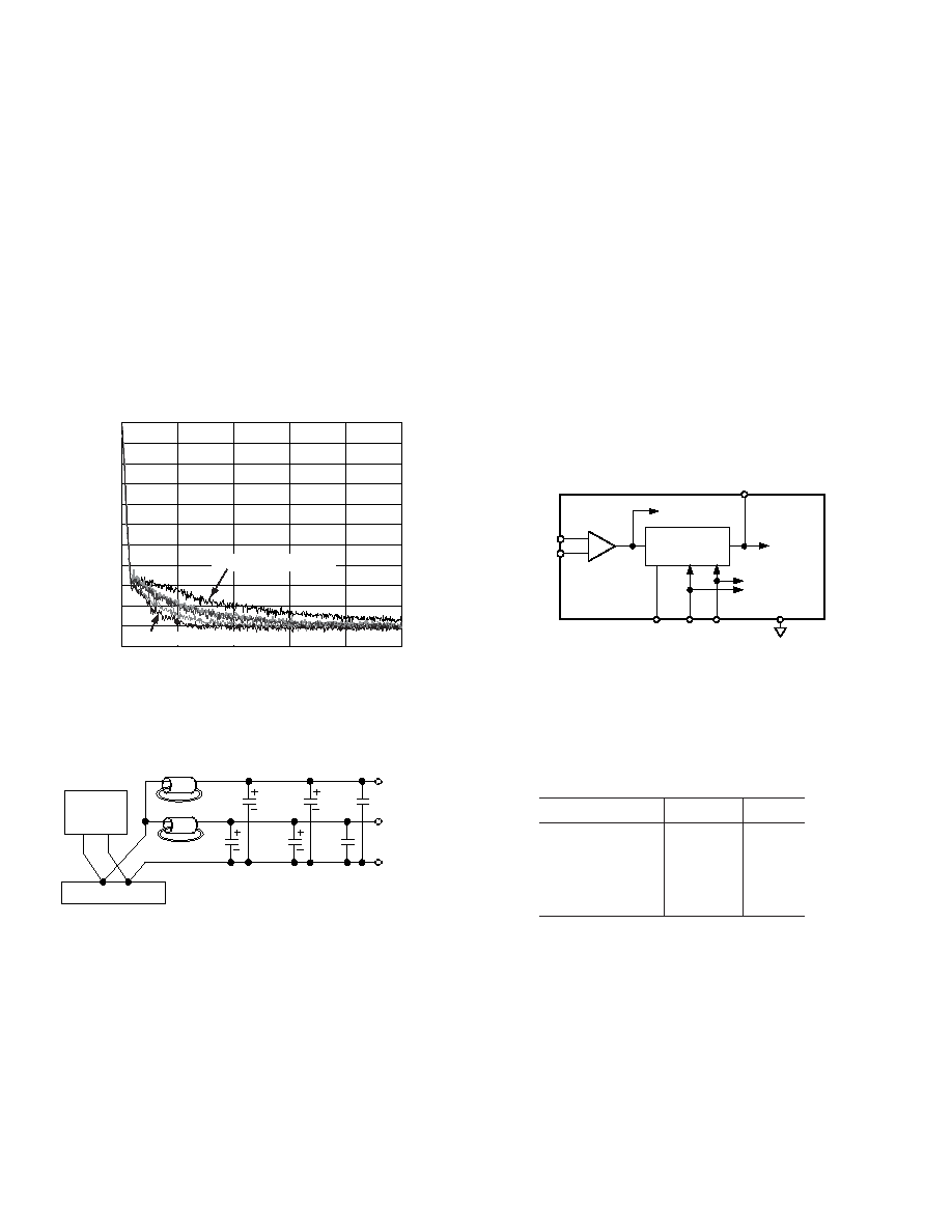
The effects of phase noise on the AD9753’s SNR performance
become more noticeable at higher reconstructed output frequen-
cies and signal levels. Figure 8 compares the phase noise of a
full-scale sine wave at exactly fDATA/4 at different data rates
(thus carrier frequency) with the optimum DIV1, DIV0 setting.
SNR is partly a function of the jitter generated by the clock
circuitry. As a result, any noise on PLLVDD or CLKVDD may
decrease the SNR at the output of the DAC. To minimize this
potential problem, PLLVDD and CLKVDD can be connected
to DVDD using an LC filter network similar to the one shown
in Figure 9.
FREQUENCY OFFSET (MHz)
0
–20
–110
5
1
0
NOISE
DENSITY
(dBm/Hz)
–10
–30
–40
–50
–60
–70
–80
–90
–100
234
PLL ON, fDATA = 150MSPS
PLL OFF, fDATA = 50MSPS
Figure 8. Phase Noise of PLL Clock Multiplier at
fOUT = fDATA/4 at Different fDATA Settings with DIV0/DIV1
Optimized, Using R&S FSEA30 Spectrum Analyzer
100 F
ELECT.
10 F
TANT.
0.1 F
CER.
TTL/CMOS
LOGIC
CIRCUITS
3.3V POWER SUPPLY
FERRITE
BEADS
CLKVDD
PLLVDD
CLKCOM
Figure 9. LC Network for Power Filtering
DAC TIMING WITH PLL ACTIVE
As described in Figure 7, in PLL active mode, Port 1 and
Port 2 input latches are updated on the rising edge of CLK. On
the same rising edge, data previously present in the input Port 2
latch is written to the DAC output latch. The DAC output will
update after a short propagation delay (tPD).
Following the rising edge of CLK at a time equal to half of its
period, the data in the Port 1 latch will be written to the DAC
output latch, again with a corresponding change in the DAC
output. Due to the internal PLL, the time at which the data in
the Port 1 and Port 2 input latches is written to the DAC latch
is independent of the duty cycle of CLK. When using the PLL,
the external clock can be operated at any duty cycle that meets
the specified input pulsewidth.
On the next rising edge of CLK, the cycle begins again with the
two input port latches being updated, and the DAC output latch
being updated with the current data in the Port 2 input latch.
PLL DISABLED MODE
When PLLVDD is grounded, the PLL is disabled. An external
clock must now drive the CLK inputs at the desired DAC out-
put update rate. The speed and timing of the data present at
input Ports 1 and 2 are now dependent on whether or not the
AD9753 is interleaving the digital input data or only responding
to data on a single port. Figure 10 is a functional block diagram
of the AD9753 clock control circuitry with the PLL disabled.
PLLVDD
TO DAC
LATCH
PLLLOCK
CLOCK
LOGIC
( 1 OR
2)
DIFFERENTIAL-
TO-
SINGLE-ENDED
AMP
TO
INTERNAL
MUX
CLKIN+
CLKIN–
AD9753
RESET DIV0 DIV1
TO INPUT
LATCHES
Figure 10. Clock Circuitry with PLL Disabled
DIV0 and DIV1 no longer control the PLL but are used to set
the control on the input mux for either interleaving or non-
interleaving the input data. The different modes for states of
DIV0 and DIV1 are given in Table II.
Table II. Input Mode for DIV0,
DIV1 Levels with PLL Disabled
Input Mode
DIV1
DIV0
Interleaved (2
×)0
0
Noninterleaved
Port 1 Selected
0
1
Port 2 Selected
1
0
Not Allowed
1
相关PDF资料 |
PDF描述 |
|---|---|
| AD9751-EB | BOARD EVAL FOR AD9751 |
| MLG1005S10NJ | INDUCTOR MULTILAYER 10NH 0402 |
| GCM10DCMT-S288 | CONN EDGECARD 20POS .156 EXTEND |
| UPB2E271MRD | CAP ALUM 270UF 250V 20% RADIAL |
| ECE-V1EA101P | CAP ALUM 100UF 25V 20% SMD |
相关代理商/技术参数 |
参数描述 |
|---|---|
| AD9754 | 制造商:AD 制造商全称:Analog Devices 功能描述:14-Bit, 125 MSPS High Performance TxDAC D/A Converter |
| AD9754AR | 功能描述:IC DAC 14BIT 125MSPS HP 28-SOIC RoHS:否 类别:集成电路 (IC) >> 数据采集 - 数模转换器 系列:TxDAC® 产品培训模块:Data Converter Fundamentals DAC Architectures 标准包装:750 系列:- 设置时间:7µs 位数:16 数据接口:并联 转换器数目:1 电压电源:双 ± 功率耗散(最大):100mW 工作温度:0°C ~ 70°C 安装类型:表面贴装 封装/外壳:28-LCC(J 形引线) 供应商设备封装:28-PLCC(11.51x11.51) 包装:带卷 (TR) 输出数目和类型:1 电压,单极;1 电压,双极 采样率(每秒):143k |
| AD9754ARRL | 制造商:Analog Devices 功能描述:DAC 1-CH 14-bit 28-Pin SOIC W T/R 制造商:Rochester Electronics LLC 功能描述:14-BIT, 125 MSPS+ TXDAC D/A CONVERTER - Tape and Reel |
| AD9754ARU | 功能描述:IC DAC 14BIT 125MSPS 28-TSSOP RoHS:否 类别:集成电路 (IC) >> 数据采集 - 数模转换器 系列:TxDAC® 产品培训模块:Data Converter Fundamentals DAC Architectures 标准包装:750 系列:- 设置时间:7µs 位数:16 数据接口:并联 转换器数目:1 电压电源:双 ± 功率耗散(最大):100mW 工作温度:0°C ~ 70°C 安装类型:表面贴装 封装/外壳:28-LCC(J 形引线) 供应商设备封装:28-PLCC(11.51x11.51) 包装:带卷 (TR) 输出数目和类型:1 电压,单极;1 电压,双极 采样率(每秒):143k |
发布紧急采购,3分钟左右您将得到回复。