参数资料
| 型号: | AD9760ARU50 |
| 厂商: | Analog Devices Inc |
| 文件页数: | 6/23页 |
| 文件大小: | 0K |
| 描述: | IC DAC 10BIT 50MSPS 28-TSSOP |
| 产品培训模块: | Data Converter Fundamentals DAC Architectures |
| 标准包装: | 50 |
| 系列: | TxDAC® |
| 设置时间: | 35ns |
| 位数: | 10 |
| 转换器数目: | 1 |
| 电压电源: | 模拟和数字 |
| 功率耗散(最大): | 175mW |
| 工作温度: | -40°C ~ 85°C |
| 安装类型: | 表面贴装 |
| 封装/外壳: | 28-TSSOP(0.173",4.40mm 宽) |
| 供应商设备封装: | 28-TSSOP |
| 包装: | 管件 |
| 输出数目和类型: | 2 电流,单极;2 电流,双极 |
| 采样率(每秒): | 60M |
| 配用: | AD9760-EBZ-ND - BOARD EVAL FOR AD9760 |
AD9760
–14–
REV. B
The enhancement in distortion performance becomes more
significant as the frequency content of the reconstructed wave-
form increases. This is due to the first order cancellation of
various dynamic common-mode distortion mechanisms, digi-
tal feedthrough and noise.
Performing a differential-to-single-ended conversion via a
transformer also provides the ability to deliver twice the re-
constructed signal power to the load (i.e., assuming no source
termination). Since the output currents of IOUTA and IOUTB are
complementary, they become additive when processed differ-
entially. A properly selected transformer will allow the AD9760
to provide the required power and voltage levels to different
loads. Refer to Applying the AD9760 section for examples of
various output configurations.
The output impedance of IOUTA and IOUTB is determined by the
equivalent parallel combination of the PMOS switches associ-
ated with the current sources and is typically 100 k
in parallel
with 5 pF. It is also slightly dependent on the output voltage
(i.e., VOUTA and VOUTB) due to the nature of a PMOS device.
As a result, maintaining IOUTA and/or IOUTB at a virtual ground
via an I-V op amp configuration will result in the optimum dc
linearity. Note the INL/DNL specifications for the AD9760 are
measured with IOUTA maintained at a virtual ground via an
op amp.
IOUTA and IOUTB also have a negative and positive voltage com-
pliance range that must be adhered to in order to achieve opti-
mum performance. The negative output compliance range of
–1.0 V is set by the breakdown limits of the CMOS process.
Operation beyond this maximum limit may result in a break-
down of the output stage and affect the reliability of the AD9760.
The positive output compliance range is slightly dependent on
the full-scale output current, IOUTFS. It degrades slightly from
its nominal 1.25 V for an IOUTFS = 20 mA to 1.00 V for an
IOUTFS = 2 mA. The optimum distortion performance for a
single-ended or differential output is achieved when the maximum
full-scale signal at IOUTA and IOUTB does not exceed 0.5 V. Ap-
plications requiring the AD9760’s output (i.e., VOUTA and/or
VOUTB) to extend its output compliance range should size RLOAD
accordingly. Operation beyond this compliance range will ad-
versely affect the AD9760’s linearity performance and subse-
quently degrade its distortion performance.
DIGITAL INPUTS
The AD9760’s digital input consists of 10 data input pins and a
clock input pin. The 10-bit parallel data inputs follow standard
positive binary coding where DB9 is the most significant bit
(MSB) and DB0 is the least significant bit (LSB). IOUTA pro-
duces a full-scale output current when all data bits are at
Logic 1. IOUTB produces a complementary output with the full-
scale current split between the two outputs as a function of the
input code.
The digital interface is implemented using an edge-triggered
master slave latch. The DAC output is updated following the
rising edge of the clock as shown in Figure 1 and is designed to
support a clock rate as high as 125 MSPS. The clock can be
operated at any duty cycle that meets the specified latch pulse-
width. The setup and hold times can also be varied within the
clock cycle as long as the specified minimum times are met
although the location of these transition edges may affect digital
feedthrough and distortion performance. Best performance is
typically achieved when the input data transitions on the falling edge
of a 50% duty cycle clock.
The digital inputs are CMOS compatible with logic thresholds,
VTHRESHOLD set to approximately half the digital positive supply
(DVDD) or
VTHRESHOLD = DVDD/2 (
±20%)
The internal digital circuitry of the AD9760 is capable of oper-
ating over a digital supply range of 2.7 V to 5.5 V. As a result,
the digital inputs can also accommodate TTL levels when
DVDD is set to accommodate the maximum high level voltage
VOH(MAX). A DVDD of 3 V to 3.3 V will typically ensure proper
compatibility with most TTL logic families. Figure 46 shows the
equivalent digital input circuit for the data and clock inputs.
The sleep mode input is similar with the exception that it con-
tains an active pull-down circuit, ensuring that the AD9760
remains enabled if this input is left disconnected.
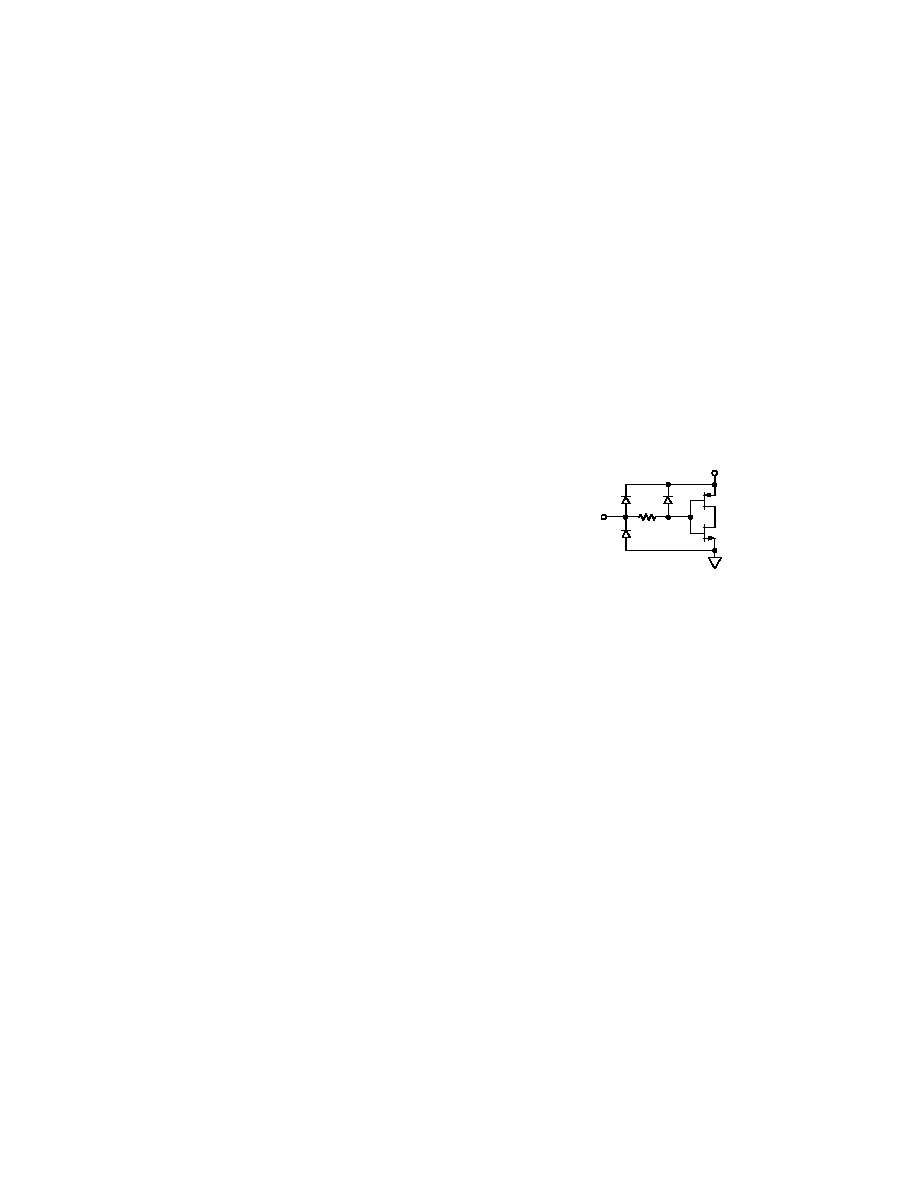
DVDD
DIGITAL
INPUT
Figure 46. Equivalent Digital Input
Since the AD9760 is capable of being updated up to 125 MSPS,
the quality of the clock and data input signals are important in
achieving the optimum performance. The drivers of the digital
data interface circuitry should be specified to meet the mini-
mum setup and hold times of the AD9760 as well as its required
min/max input logic level thresholds. Typically, the selection of
the slowest logic family that satisfies the above conditions will
result in the lowest data feedthrough and noise.
Digital signal paths should be kept short and run lengths
matched to avoid propagation delay mismatch. The insertion of
a low value resistor network (i.e., 20
to 100 ) between the
AD9760 digital inputs and driver outputs may be helpful in
reducing any overshooting and ringing at the digital inputs that
contribute to data feedthrough. For longer run lengths and high
data update rates, strip line techniques with proper termination
resistors should be considered to maintain “clean” digital in-
puts. Also, operating the AD9760 with reduced logic swings and
a corresponding digital supply (DVDD) will also reduce data
feedthrough.
The external clock driver circuitry should provide the AD9760
with a low jitter clock input meeting the min/max logic levels
while providing fast edges. Fast clock edges will help minimize
any jitter that will manifest itself as phase noise on a recon-
structed waveform. Thus, the clock input should be driven by
the fastest logic family suitable for the application.
相关PDF资料 |
PDF描述 |
|---|---|
| AD7533JP | IC DAC 10BIT MULTIPLYING 20-PLCC |
| V300A48H400BF2 | CONVERTER MOD DC/DC 48V 400W |
| LTC2753IUK-12#PBF | IC DAC 12BIT DUAL 48-QFN |
| V300A3V3H264BL | CONVERTER MOD DC/DC 3.3V 264W |
| AD421BRZRL | IC DAC 16BIT LOOP 4-20MA 16SOIC |
相关代理商/技术参数 |
参数描述 |
|---|---|
| AD9760ARU50RL | 功能描述:INTEGRATED CIRCUIT 制造商:analog devices inc. 系列:* 包装:带卷(TR) 零件状态:最後搶購 封装/外壳:28-TSSOP(0.173",4.40mm 宽) 供应商器件封装:28-TSSOP 标准包装:1 |
| AD9760ARU50RL7 | 功能描述:IC DAC 10BIT 50MSPS 28-TSSOP RoHS:否 类别:集成电路 (IC) >> 数据采集 - 数模转换器 系列:TxDAC® 标准包装:47 系列:- 设置时间:2µs 位数:14 数据接口:并联 转换器数目:1 电压电源:单电源 功率耗散(最大):55µW 工作温度:-40°C ~ 85°C 安装类型:表面贴装 封装/外壳:28-SSOP(0.209",5.30mm 宽) 供应商设备封装:28-SSOP 包装:管件 输出数目和类型:1 电流,单极;1 电流,双极 采样率(每秒):* |
| AD9760ARURL | 功能描述:INTEGRATED CIRCUIT 制造商:analog devices inc. 系列:* 包装:带卷(TR) 零件状态:最後搶購 封装/外壳:28-TSSOP(0.173",4.40mm 宽) 供应商器件封装:28-TSSOP 标准包装:1 |
| AD9760ARURL7 | 制造商:Analog Devices 功能描述:DAC 1-CH 10-bit 28-Pin TSSOP T/R 制造商:Rochester Electronics LLC 功能描述:- Bulk |
| AD9760ARUZ | 功能描述:IC DAC 10BIT 125MSPS 28-TSSOP RoHS:是 类别:集成电路 (IC) >> 数据采集 - 数模转换器 系列:TxDAC® 产品培训模块:Lead (SnPb) Finish for COTS Obsolescence Mitigation Program 标准包装:50 系列:- 设置时间:4µs 位数:12 数据接口:串行 转换器数目:2 电压电源:单电源 功率耗散(最大):- 工作温度:-40°C ~ 85°C 安装类型:表面贴装 封装/外壳:8-TSSOP,8-MSOP(0.118",3.00mm 宽) 供应商设备封装:8-uMAX 包装:管件 输出数目和类型:2 电压,单极 采样率(每秒):* 产品目录页面:1398 (CN2011-ZH PDF) |
发布紧急采购,3分钟左右您将得到回复。