参数资料
| 型号: | AD9760ARZ |
| 厂商: | Analog Devices Inc |
| 文件页数: | 10/23页 |
| 文件大小: | 0K |
| 描述: | IC DAC 10BIT 125MSPS 28-SOIC |
| 产品培训模块: | Data Converter Fundamentals DAC Architectures |
| 标准包装: | 27 |
| 系列: | TxDAC® |
| 设置时间: | 35ns |
| 位数: | 10 |
| 转换器数目: | 1 |
| 电压电源: | 模拟和数字 |
| 功率耗散(最大): | 175mW |
| 工作温度: | -40°C ~ 85°C |
| 安装类型: | 表面贴装 |
| 封装/外壳: | 28-SOIC(0.295",7.50mm 宽) |
| 供应商设备封装: | 28-SOIC |
| 包装: | 管件 |
| 输出数目和类型: | 2 电流,单极;2 电流,双极 |
| 采样率(每秒): | 125M |
| 配用: | AD9760-EBZ-ND - BOARD EVAL FOR AD9760 |
AD9760
–18–
REV. B
APPLICATIONS
Using the AD9760 for QAM Modulation
QAM is one of the most widely used digital modulation schemes
in digital communication systems. This modulation technique
can be found in both FDM spreadspectrum (i.e., CDMA) based
systems. A QAM signal is a carrier frequency that is both
modulated in amplitude (i.e., AM modulation) and in phase
(i.e., PM modulation). It can be generated by independently
modulating two carriers of identical frequency but with a 90
°
phase difference. This results in an in-phase (I) carrier compo-
nent and a quadrature (Q) carrier component at a 90
° phase
shift with respect to the I component. The I and Q components
are then summed to provide a QAM signal at the specified car-
rier frequency.
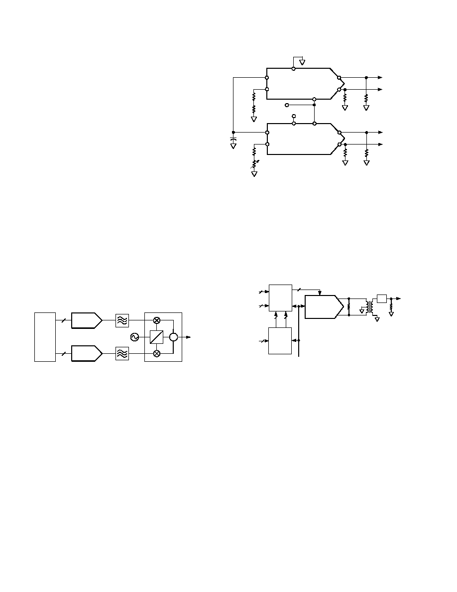
A common and traditional implementation of a QAM modu-
lator is shown in Figure 56. The modulation is performed in the
analog domain in which two DACs are used to generate the
baseband I and Q components, respectively. Each component is
then typically applied to a Nyquist filter before being applied to
a quadrature mixer. The matching Nyquist filters shape and
limit each component’s spectral envelope while minimizing
intersymbol interference. The DAC is typically updated at the
QAM symbol rate or possibly a multiple of it if an interpolating
filter precedes the DAC. The use of an interpolating filter typi-
cally eases the implementation and complexity of the analog
filter, which can be a significant contributor to mismatches in
gain and phase between the two baseband channels. A quadra-
ture mixer modulates the I and Q components with in-phase
and quadrature phase carrier frequency and sums the two out-
puts to provide the QAM signal.
AD9760
0
90
Σ
AD9760
CARRIER
FREQUENCY
10
TO
MIXER
DSP
OR
ASIC
NYQUIST
FILTERS
QUADRATURE
MODULATOR
Figure 56. Typical Analog QAM Architecture
In this implementation, it is much more difficult to maintain
proper gain and phase matching between the I and Q channels.
The circuit implementation shown in Figure 57 helps improve
on the matching and temperature stability characteristics be-
tween the I and Q channels. Using a single voltage reference
derived from U1 to set the gain for both the I and Q channels
will improve the gain matching and stability. Further enhance-
ments in gain matching and stability are achieved by using sepa-
rate matching resistor networks for both RSET and RLOAD.
Additional trim capability via RCAL1 and RCAL2 can be added to
compensate for any initial mismatch in gain between the two
channels. This may be attributed to any mismatch between U1
and U2’s gain setting resistor (RSET), effective load resistance,
(RLOAD), and/or voltage offset of each DAC’s control amplifier.
The differential voltage outputs of U1 and U2 are fed into their
respective differential inputs of a quadrature mixer via matching
50
filter networks.
It is also possible to generate a QAM signal completely in the
digital domain via a DSP or ASIC, in which case only a single
DAC of sufficient resolution and performance is required to
reconstruct the QAM signal. Also available from several vendors
REFIO
FS ADJ
IOUTA
IOUTB
CLOCK
RSET
2k *
RCAL1
50
CLOCK
U1
I-CHANNEL
50 **
RLOAD
50 **
RLOAD
TO
NYQUIST
FILTER
AND MIXER
REFIO
FS ADJ
IOUTA
IOUTB
CLOCK
RSET
2k *
RCAL2
100
U2
Q-CHANNEL
50 **
RLOAD
50 **
RLOAD
TO
NYQUIST
FILTER
AND MIXER
0.1 F
REFLO
AVDD
* OHMTEK ORNA1001F
** OHMTEK TOMC1603-50F
Figure 57. Baseband QAM Implementation Using Two
AD9760s
are Digital ASICs which implement other digital modulation
schemes such as PSK and FSK. This digital implementation has
the benefit of generating perfectly matched I and Q components
in terms of gain and phase, which is essential in maintaining
optimum performance in a communication system. In this
implementation, the reconstruction DAC must be operating at a
sufficiently high clock rate to accommodate the highest specified
QAM carrier frequency. Figure 58 shows a block diagram of
such an implementation using the AD9760.
50
AD9760
LPF
50
TO
MIXER
STEL-1130
QAM
12
COS
12
SIN
12
I DATA
Q DATA
12
CARRIER
FREQUENCY
10
STEL-1177
NCO
CLOCK
Figure 58. Digital QAM Architecture
AD9760 EVALUATION BOARD
General Description
The AD9760-EB is an evaluation board for the AD9760 10-bit
D/A converter. Careful attention to layout and circuit design,
combined with a prototyping area, allow the user to easily and
effectively evaluate the AD9760 in any application where high
resolution, high speed conversion is required.
This board allows the user the flexibility to operate the AD9760
in various configurations. Possible output configurations include
transformer coupled, resistor terminated, inverting/noninverting
and differential amplifier outputs. The digital inputs are designed
to be driven directly from various word generators with the on-
board option to add a resistor network for proper load termina-
tion. Provisions are also made to operate the AD9760 with
either the internal or external reference or to exercise the power-
down feature.
Refer to the application note AN-420, “Using the AD9760/
AD9760/AD9764-EB Evaluation Board,” for a thorough
description and operating instructions for the AD9760 evalua-
tion board.
相关PDF资料 |
PDF描述 |
|---|---|
| VI-BNB-MV-B1 | CONVERTER MOD DC/DC 95V 150W |
| PI49FCT3807CS | IC CLK BUFFER 1:10 100MHZ 20SOIC |
| PI49FCT3807CQ | IC CLK BUFFER 1:10 100MHZ 20QSOP |
| LTC1446LIS8#PBF | IC D/A CONV 12BIT R-R DUAL 8SOIC |
| PI49FCT805ATS | IC CLOCK BUFFER 1:5 66MHZ 20SOIC |
相关代理商/技术参数 |
参数描述 |
|---|---|
| AD9760ARZ50 | 功能描述:IC DAC 10BIT 50MSPS 28-SOIC RoHS:是 类别:集成电路 (IC) >> 数据采集 - 数模转换器 系列:TxDAC® 标准包装:47 系列:- 设置时间:2µs 位数:14 数据接口:并联 转换器数目:1 电压电源:单电源 功率耗散(最大):55µW 工作温度:-40°C ~ 85°C 安装类型:表面贴装 封装/外壳:28-SSOP(0.209",5.30mm 宽) 供应商设备封装:28-SSOP 包装:管件 输出数目和类型:1 电流,单极;1 电流,双极 采样率(每秒):* |
| AD9760ARZ50RL | 功能描述:IC DAC 10BIT 125MSPS 28TSSOP RoHS:是 类别:集成电路 (IC) >> 数据采集 - 数模转换器 系列:TxDAC® 标准包装:47 系列:- 设置时间:2µs 位数:14 数据接口:并联 转换器数目:1 电压电源:单电源 功率耗散(最大):55µW 工作温度:-40°C ~ 85°C 安装类型:表面贴装 封装/外壳:28-SSOP(0.209",5.30mm 宽) 供应商设备封装:28-SSOP 包装:管件 输出数目和类型:1 电流,单极;1 电流,双极 采样率(每秒):* |
| AD9760ARZRL | 功能描述:IC DAC 10BIT 125MSPS 28-SOIC RoHS:是 类别:集成电路 (IC) >> 数据采集 - 数模转换器 系列:TxDAC® 标准包装:47 系列:- 设置时间:2µs 位数:14 数据接口:并联 转换器数目:1 电压电源:单电源 功率耗散(最大):55µW 工作温度:-40°C ~ 85°C 安装类型:表面贴装 封装/外壳:28-SSOP(0.209",5.30mm 宽) 供应商设备封装:28-SSOP 包装:管件 输出数目和类型:1 电流,单极;1 电流,双极 采样率(每秒):* |
| AD9760-EB | 制造商:Analog Devices 功能描述: 制造商:Rochester Electronics LLC 功能描述: |
| AD9760-EBZ | 功能描述:BOARD EVAL FOR AD9760 RoHS:是 类别:编程器,开发系统 >> 评估板 - 数模转换器 (DAC) 系列:TxDAC® 产品培训模块:Lead (SnPb) Finish for COTS Obsolescence Mitigation Program 标准包装:1 系列:- DAC 的数量:4 位数:12 采样率(每秒):- 数据接口:串行,SPI? 设置时间:3µs DAC 型:电流/电压 工作温度:-40°C ~ 85°C 已供物品:板 已用 IC / 零件:MAX5581 |
发布紧急采购,3分钟左右您将得到回复。