参数资料
| 型号: | AD9760ARZ |
| 厂商: | Analog Devices Inc |
| 文件页数: | 4/23页 |
| 文件大小: | 0K |
| 描述: | IC DAC 10BIT 125MSPS 28-SOIC |
| 产品培训模块: | Data Converter Fundamentals DAC Architectures |
| 标准包装: | 27 |
| 系列: | TxDAC® |
| 设置时间: | 35ns |
| 位数: | 10 |
| 转换器数目: | 1 |
| 电压电源: | 模拟和数字 |
| 功率耗散(最大): | 175mW |
| 工作温度: | -40°C ~ 85°C |
| 安装类型: | 表面贴装 |
| 封装/外壳: | 28-SOIC(0.295",7.50mm 宽) |
| 供应商设备封装: | 28-SOIC |
| 包装: | 管件 |
| 输出数目和类型: | 2 电流,单极;2 电流,双极 |
| 采样率(每秒): | 125M |
| 配用: | AD9760-EBZ-ND - BOARD EVAL FOR AD9760 |
AD9760
–12–
REV. B
The differential voltage, VDIFF, appearing across IOUTA and
IOUTB is:
VDIFF = (IOUTA – IOUTB)
× RLOAD
(7)
Substituting the values of IOUTA, IOUTB and IREF; VDIFF can be
expressed as:
VDIFF = {(2 DAC CODE – 1023)/1024}
×
(32 RLOAD/RSET)
× V
REFIO
(8)
These last two equations highlight some of the advantages of
operating the AD9760 differentially. First, the differential op-
eration will help cancel common-mode error sources associated
with IOUTA and IOUTB such as noise, distortion and dc offsets.
Second, the differential code dependent current and subsequent
voltage, VDIFF, is twice the value of the single-ended voltage
output (i.e., VOUTA or VOUTB), thus providing twice the signal
power to the load.
Note, the gain drift temperature performance for a single-ended
(VOUTA and VOUTB) or differential output (VDIFF) of the AD9760
can be enhanced by selecting temperature tracking resistors for
RLOAD and RSET due to their ratiometric relationship as shown
in Equation 8.
REFERENCE OPERATION
The AD9760 contains an internal 1.20 V bandgap reference
that can be easily disabled and overridden by an external refer-
ence. REFIO serves as either an input or output depending on
whether the internal or an external reference is selected. If
REFLO is tied to ACOM, as shown in Figure 40, the internal
reference is activated and REFIO provides a 1.20 V output. In
this case, the internal reference must be compensated externally
with a ceramic chip capacitor of 0.1
F or greater from REFIO
to REFLO. Also, REFIO should be buffered with an external
amplifier having an input bias current less than 100 nA if any
additional loading is required.
50pF
COMP1
+1.2V REF
AVDD
REFLO
CURRENT
SOURCE
ARRAY
0.1 F
+5V
REFIO
FS ADJ
2k
0.1 F
AD9760
ADDITIONAL
LOAD
OPTIONAL
EXTERNAL
REF BUFFER
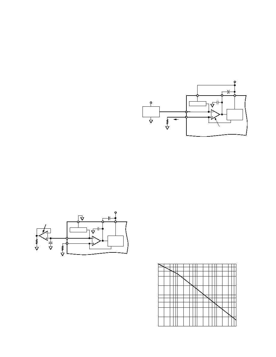
Figure 40. Internal Reference Configuration
The internal reference can be disabled by connecting REFLO to
AVDD. In this case, an external reference may be applied to
REFIO as shown in Figure 41. The external reference may
provide either a fixed reference voltage to enhance accuracy and
drift performance or a varying reference voltage for gain control.
Note that the 0.1
F compensation capacitor is not required
since the internal reference is disabled, and the high input im-
pedance (i.e., 1 M
) of REFIO minimizes any loading of the
external reference.
REFERENCE CONTROL AMPLIFIER
The AD9760 also contains an internal control amplifier that is
used to regulate the DAC’s full-scale output current, IOUTFS.
The control amplifier is configured as a V-I converter as shown
in Figure 41, so that its current output, IREF, is determined by
the ratio of the VREFIO and an external resistor, RSET, as stated
in Equation 4. IREF is copied over to the segmented current
sources with the proper scaling factor to set IOUTFS as stated in
Equation 3.
50pF
COMP1
+1.2V REF
AVDD
REFLO
CURRENT
SOURCE
ARRAY
0.1 F
AVDD
REFIO
FS ADJ
RSET
AD9760
EXTERNAL
REF
IREF =
VREFIO/RSET
AVDD
REFERENCE
CONTROL
AMPLIFIER
VREFIO
Figure 41. External Reference Configuration
The control amplifier allows a wide (10:1) adjustment span of
IOUTFS over a 2 mA to 20 mA range by setting IREF between
62.5
A and 625 A. The wide adjustment span of I
OUTFS pro-
vides several application benefits. The first benefit relates
directly to the power dissipation of the AD9760, which is
proportional to IOUTFS (refer to the Power Dissipation section).
The second benefit relates to the 20 dB adjustment, which is
useful for system gain control purposes.
The small signal bandwidth of the reference control amplifier is
approximately 1.4 MHz and can be reduced by connecting an
external capacitor between COMP1 and AVDD. The output of
the control amplifier, COMP1, is internally compensated via a
50 pF capacitor that limits the control amplifier small-signal
bandwidth and reduces its output impedance. Any additional
external capacitance further limits the bandwidth and acts as a
filter to reduce the noise contribution from the reference ampli-
fier. Figure 42 shows the relationship between the external
capacitor and the small signal –3 dB bandwidth of the refer-
ence amplifier. Since the –3 dB bandwidth corresponds to the
dominant pole, and hence the time constant, the settling time of
the control amplifier to a stepped reference input response can
be approximated.
COMP1 CAPACITOR – nF
1000
10
0.1
1000
1
BANDWIDTH
–
kHz
10
100
Figure 42. External COMP1 Capacitor vs. –3 dB Bandwidth
相关PDF资料 |
PDF描述 |
|---|---|
| VI-BNB-MV-B1 | CONVERTER MOD DC/DC 95V 150W |
| PI49FCT3807CS | IC CLK BUFFER 1:10 100MHZ 20SOIC |
| PI49FCT3807CQ | IC CLK BUFFER 1:10 100MHZ 20QSOP |
| LTC1446LIS8#PBF | IC D/A CONV 12BIT R-R DUAL 8SOIC |
| PI49FCT805ATS | IC CLOCK BUFFER 1:5 66MHZ 20SOIC |
相关代理商/技术参数 |
参数描述 |
|---|---|
| AD9760ARZ50 | 功能描述:IC DAC 10BIT 50MSPS 28-SOIC RoHS:是 类别:集成电路 (IC) >> 数据采集 - 数模转换器 系列:TxDAC® 标准包装:47 系列:- 设置时间:2µs 位数:14 数据接口:并联 转换器数目:1 电压电源:单电源 功率耗散(最大):55µW 工作温度:-40°C ~ 85°C 安装类型:表面贴装 封装/外壳:28-SSOP(0.209",5.30mm 宽) 供应商设备封装:28-SSOP 包装:管件 输出数目和类型:1 电流,单极;1 电流,双极 采样率(每秒):* |
| AD9760ARZ50RL | 功能描述:IC DAC 10BIT 125MSPS 28TSSOP RoHS:是 类别:集成电路 (IC) >> 数据采集 - 数模转换器 系列:TxDAC® 标准包装:47 系列:- 设置时间:2µs 位数:14 数据接口:并联 转换器数目:1 电压电源:单电源 功率耗散(最大):55µW 工作温度:-40°C ~ 85°C 安装类型:表面贴装 封装/外壳:28-SSOP(0.209",5.30mm 宽) 供应商设备封装:28-SSOP 包装:管件 输出数目和类型:1 电流,单极;1 电流,双极 采样率(每秒):* |
| AD9760ARZRL | 功能描述:IC DAC 10BIT 125MSPS 28-SOIC RoHS:是 类别:集成电路 (IC) >> 数据采集 - 数模转换器 系列:TxDAC® 标准包装:47 系列:- 设置时间:2µs 位数:14 数据接口:并联 转换器数目:1 电压电源:单电源 功率耗散(最大):55µW 工作温度:-40°C ~ 85°C 安装类型:表面贴装 封装/外壳:28-SSOP(0.209",5.30mm 宽) 供应商设备封装:28-SSOP 包装:管件 输出数目和类型:1 电流,单极;1 电流,双极 采样率(每秒):* |
| AD9760-EB | 制造商:Analog Devices 功能描述: 制造商:Rochester Electronics LLC 功能描述: |
| AD9760-EBZ | 功能描述:BOARD EVAL FOR AD9760 RoHS:是 类别:编程器,开发系统 >> 评估板 - 数模转换器 (DAC) 系列:TxDAC® 产品培训模块:Lead (SnPb) Finish for COTS Obsolescence Mitigation Program 标准包装:1 系列:- DAC 的数量:4 位数:12 采样率(每秒):- 数据接口:串行,SPI? 设置时间:3µs DAC 型:电流/电压 工作温度:-40°C ~ 85°C 已供物品:板 已用 IC / 零件:MAX5581 |
发布紧急采购,3分钟左右您将得到回复。