参数资料
| 型号: | AD9761ARSZ |
| 厂商: | Analog Devices Inc |
| 文件页数: | 3/24页 |
| 文件大小: | 0K |
| 描述: | IC DAC 10BIT DUAL 40MSPS 28-SSOP |
| 产品培训模块: | Data Converter Fundamentals DAC Architectures |
| 标准包装: | 47 |
| 设置时间: | 35ns |
| 位数: | 10 |
| 数据接口: | 并联 |
| 转换器数目: | 2 |
| 电压电源: | 模拟和数字 |
| 功率耗散(最大): | 250mW |
| 工作温度: | -40°C ~ 85°C |
| 安装类型: | 表面贴装 |
| 封装/外壳: | 28-SSOP(0.209",5.30mm 宽) |
| 供应商设备封装: | 28-SSOP |
| 包装: | 管件 |
| 输出数目和类型: | 4 电流,单极;4 电流,双极 |
| 采样率(每秒): | 40M |
| 产品目录页面: | 785 (CN2011-ZH PDF) |
| 配用: | AD9761-EBZ-ND - BOARD EVAL FOR AD9761 |
AD9761
–10–
AD9761
–11–
log filter is typically determined by the proximity of the desired
fundamental to the first image and the required amount of image
suppression.
Referring to Figure 5, the “new” first image associated with the
DAC’s higher data rate after interpolation is “pushed” out fur-
ther relative to the input signal. The “old” first image associated
with the lower DAC data rate before interpolation is suppressed
by the digital filter. As a result, the transition band for the analog
reconstruction filter is increased, thus reducing the complexity
of the analog filter.
The digital interpolation filters for I and Q paths are identi-
cal 43-tap half-band symmetric FIR filters. Each filter receives
de-interleaved I or Q data from the digital input interface. The
input CLOCK signal is internally divided by 2 to generate the
filter clock.The filters are implemented with two parallel paths
running at the filter clock rate. The output from each path is
selected on opposite phases of the filter clock, thus producing
interpolated filtered output data at the input clock rate. The
frequency response and impulse response of these filters are
shown in Figures 2a and 2b. Table I lists the idealized filter
coefficients that correspond to the filter’s impulse response.
The digital section of the AD9761 also includes an input interface
section designed to support interleaved I and Q input data from
a single 10-bit bus. This section de-interleaves the I and Q input
data while ensuring its proper pairing for the 2 interpolation
filters. A RESET/SLEEP input serves a dual function by providing
a reset function for this section as well as providing power-down
functionality. Refer to the Digital Inputs and Interleaved Interface
Considerations and RESET/SLEEP Mode Operation sections for
a more detailed discussion.
DAC TRANSFER FUNCTION
Each I and Q DAC provides complementary current output
pins: IOUT(A/B) and QOUT(A/B), respectively. Note that
QOUTA and QOUTB operate identically to IOUTA and
IOUTB. IOUTA will provide a near full-scale current output,
IOUTFS, when all bits are high (i.e., DAC CODE = 1023), while
IOUTB, the complementary output, provides no current. The
current outputs of IOUTA and IOUTB are a function of both
the input code and IOUTFS and can be expressed as
I
DAC CODE/
I
OUTA
OUTFS
=
(
)×
1024
(1)
I
– DAC CODE
I
OUTB
OUTFS
=
(
)
×
1023
1024
/
(2)
where:
DAC CODE = 0 to 1023 (i.e., decimal representation).
As previously mentioned, IOUTFS is a function of the reference
current, IREF, which is nominally set by a reference, VREFIO, and
external resistor, RSET. It can be expressed as
I
OUTFS
REF
=
×
16
(3)
where:
I
V
R
REF
REFIO
SET
=
/
(4)
The two current outputs will typically drive a resistive load
directly or via a transformer. If dc coupling is required, IOUTA
and IOUTB should be directly connected to matching resistive
loads, RLOAD, which are tied to analog common, ACOM. Note
that RLOAD represents the equivalent load resistance seen by
IOUTA or IOUTB. The single-ended voltage output appearing
at IOUTA and IOUTB pins is simply
V
I
R
IOUTA
OUTA
LOAD
=
×
(5)
V
I
R
IOUTB
OUTB
LOAD
=
×
(6)
Note that the full-scale value of VIOUTA and VIOUTB should not
exceed the specified output compliance range to maintain speci-
fied distortion and linearity performance.
The differential voltage, VIDIFF, appearing across IOUTA and
IOUTB is
V
I
R
IDIFF
IOUTA
IOUTB
LOAD
=
(
)×
–
(7)
Substituting the values of IIOUTA, IIOUTB, and IREF, VIDIFF can be
expressed as
V
DAC CODE –
R
V
IDIFF
LOAD
SET
REFIO
=
(
)
{
}×
(
)×
2
1023 1024
16
/
(8)
These last two equations highlight some of the advantages of
operating the AD9761 differentially. First, differential opera-
tion will help cancel common-mode error sources associated
with IIOUTA and IIOUTB, such as noise and distortion. Second,
the differential code-dependent current and subsequent volt-
age, VIDIFF, is twice the value of the single-ended voltage output
(i.e., VIOUTA or VIOUTB), thus providing twice the signal power to
the load.
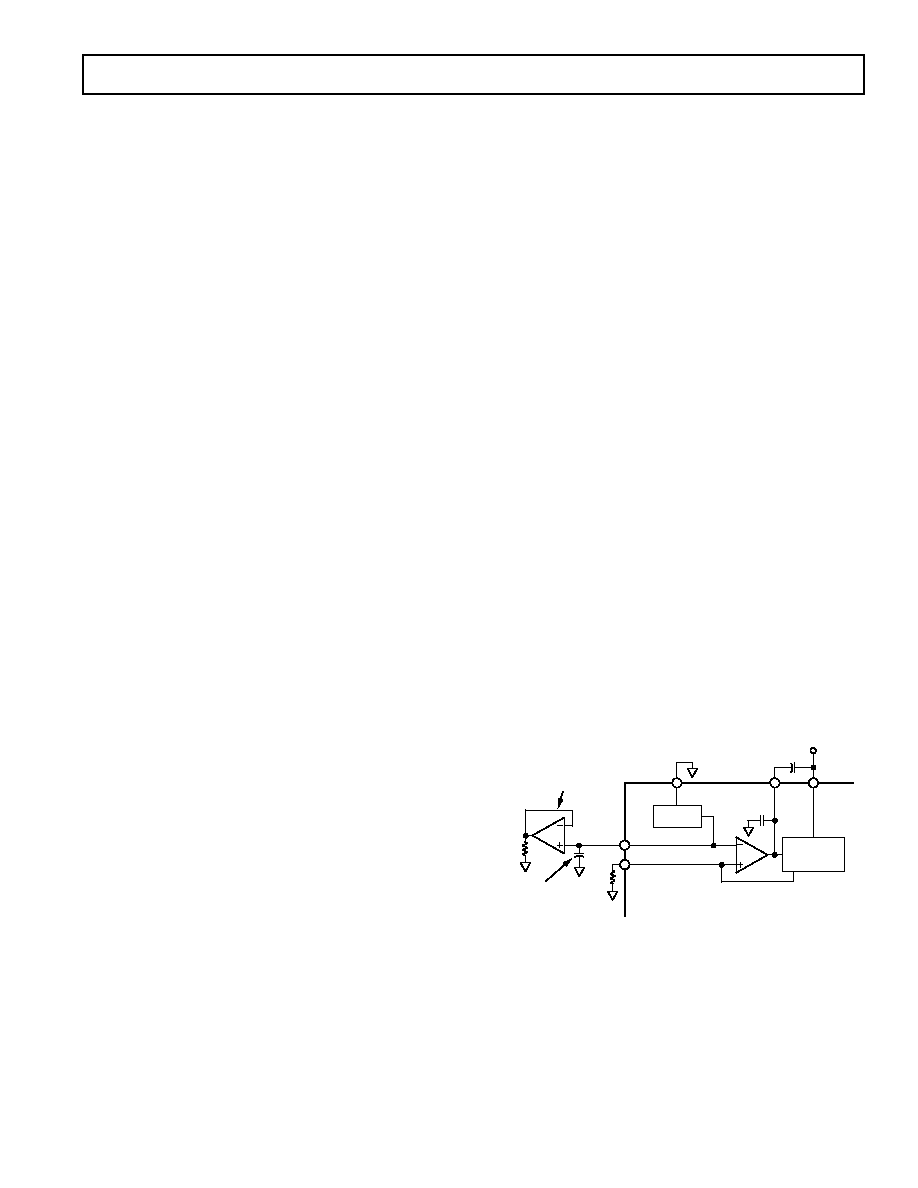
REFERENCE OPERATION
The AD9761 contains an internal 1.20 V band gap reference that
can be easily disabled and overridden by an external reference.
REFIO serves as either an input or output depending on whether
the internal or an external reference is selected. If REFLO is tied
to ACOM as shown in Figure 6, the internal reference is activated
and REFIO provides a 1.20 V output. In this case, the internal ref-
erence must be filtered externally with a ceramic chip capacitor of
0.1 F or greater from REFIO to REFLO. Also, REFIO should be
buffered with an external amplifier having a low input bias current
(i.e., <1 A) if any additional loading is required.
50pF
CURRENT
SOURCE
ARRAY
+1.2V REF
REFIO
FSADJ
REFLO
COMP2
AVDD
0.1F
RSET
2k
0.1F
OPTIONAL EXTERNAL
REF BUFFER FOR
ADDITIONAL LOADS
COMPENSATION
CAPACITOR
REQUIRED
AD9761
Figure 6. Internal Reference Configuration
The internal reference can also be disabled by connecting
REFLO to AVDD. In this case, an external reference may then
be applied to REFIO as shown in Figure 7.The external reference
may provide either a fixed reference voltage to enhance accura-
cy and drift performance or a varying reference voltage for gain
control. Note that the 0.1 F compensation capacitor is not
required since the internal reference is disabled and the high
input impedance (i.e., 1 M) of REFIO minimizes any loading
of the external reference.
REV. C
相关PDF资料 |
PDF描述 |
|---|---|
| VI-J0R-MZ-F2 | CONVERTER MOD DC/DC 7.5V 25W |
| SI5338K-A-GM | IC CLK GEN I2C BUS PROG 24QFN |
| D38999/20KF32PC | CONN RCPT 32POS WALL MNT W/PINS |
| MS3101A36-8S | CONN RCPT 47POS FREE HNG W/SCKT |
| M83723/84G1212N | CONN RCPT 12POS JAM NUT W/SCKT |
相关代理商/技术参数 |
参数描述 |
|---|---|
| AD9761ARSZRL | 功能描述:IC DAC 10BIT DUAL 40MSPS 28-SSOP RoHS:是 类别:集成电路 (IC) >> 数据采集 - 数模转换器 系列:- 标准包装:47 系列:- 设置时间:2µs 位数:14 数据接口:并联 转换器数目:1 电压电源:单电源 功率耗散(最大):55µW 工作温度:-40°C ~ 85°C 安装类型:表面贴装 封装/外壳:28-SSOP(0.209",5.30mm 宽) 供应商设备封装:28-SSOP 包装:管件 输出数目和类型:1 电流,单极;1 电流,双极 采样率(每秒):* |
| AD9761-EB | 制造商:Analog Devices 功能描述:Evaluation Board For AD9761 制造商:Analog Devices 功能描述:DEV TOOLS, EVAL BD FOR AD9761 - Bulk 制造商:Analog Devices 功能描述:SEMICONDUCTOR ((NS)) |
| AD9761-EBZ | 功能描述:BOARD EVAL FOR AD9761 RoHS:是 类别:编程器,开发系统 >> 评估板 - 数模转换器 (DAC) 系列:TxDAC® 产品培训模块:Lead (SnPb) Finish for COTS Obsolescence Mitigation Program 标准包装:1 系列:- DAC 的数量:4 位数:12 采样率(每秒):- 数据接口:串行,SPI? 设置时间:3µs DAC 型:电流/电压 工作温度:-40°C ~ 85°C 已供物品:板 已用 IC / 零件:MAX5581 |
| AD9762 | 制造商:AD 制造商全称:Analog Devices 功能描述:Analog Devices: Data Converters: DAC 12-Bit, 10 ns to 100 ns Converters Selection Table |
发布紧急采购,3分钟左右您将得到回复。