- 您现在的位置:买卖IC网 > PDF目录8631 > AD9761ARSZRL (Analog Devices Inc)IC DAC 10BIT DUAL 40MSPS 28-SSOP PDF资料下载
参数资料
| 型号: | AD9761ARSZRL |
| 厂商: | Analog Devices Inc |
| 文件页数: | 4/24页 |
| 文件大小: | 0K |
| 描述: | IC DAC 10BIT DUAL 40MSPS 28-SSOP |
| 产品培训模块: | Data Converter Fundamentals DAC Architectures |
| 标准包装: | 1,500 |
| 设置时间: | 35ns |
| 位数: | 10 |
| 数据接口: | 并联 |
| 转换器数目: | 2 |
| 电压电源: | 模拟和数字 |
| 功率耗散(最大): | 250mW |
| 工作温度: | -40°C ~ 85°C |
| 安装类型: | 表面贴装 |
| 封装/外壳: | 28-SSOP(0.209",5.30mm 宽) |
| 供应商设备封装: | 28-SSOP |
| 包装: | 带卷 (TR) |
| 输出数目和类型: | 4 电流,单极;4 电流,双极 |
| 采样率(每秒): | 40M |
| 配用: | AD9761-EBZ-ND - BOARD EVAL FOR AD9761 |
AD9761
–12–
AD9761
–13–
50pF
CURRENT
SOURCE
ARRAY
+1.2V REF
REFIO
FSADJ
REFLO
COMP2
AVDD
IREF =
VREF/RSET
AVDD
RSET
EXT.
VREF
AVDD
0.1F
AD9761
+
–
Figure 7. External Reference Configuration
REFERENCE CONTROL AMPLIFIER
The AD9761 also contains an internal control amplifier that is
used to simultaneously regulate both DACs’ full-scale output
current, IOUTFS. Since the I and Q IOUTFS are derived from
the same voltage reference and control circuitry, excellent
gain matching is ensured. The control amplifier is configured
as a V-I converter as shown in Figure 7 such that its current
output, IREF, is determined by the ratio of the VREFIO and an
external resistor, RSET, as stated in Equation 4. IREF is copied
over to the segmented current sources with the proper scaling
factor to set IOUTFS as stated in Equation 3.
The control amplifier allows a wide (10:1) adjustment span
of IOUTFS over a 1 mA to 10 mA range by setting IREF between
62.5 A and 625 A. The wide adjustment span of IOUTFS
provides several application benefits. The first benefit relates
directly to the power dissipation of the AD9761’s analog
supply, AVDD, which is proportional to IOUTFS (refer to the
Power Dissipation section). The second benefit relates to the
20 dB adjustment span, which may be useful for system gain
control purposes.
Optimum noise and dynamic performance for the AD9761 is
obtained with a 0.1 F external capacitor installed between
COMP2 and AVDD. The bandwidth of the reference control
amplifier is limited to approximately 5 kHz with a 0.1 F
capacitor installed. Since the –3 dB bandwidth corresponds
to the dominant pole and therefore its dominant time con-
stant, the settling time of the control amplifier to a stepped
reference input response can be easily determined. Note that
the output of the control amplifier, COMP2, is internally
compensated via a 50 pF capacitor, thus ensuring its stabil-
ity if no external capacitor is added.
Depending on the requirements of the application, IREF
can be adjusted by varying either RSET, or, in the external
reference mode, by varying the REFIO voltage. IREF can be
varied for a fixed RSET by disabling the internal reference and
varying the voltage of REFIO over its compliance range of
1.25 V to 0.10 V. REFIO can be driven by a single-supply
amplifier or DAC, thus allowing IREF to be varied for a fixed
RSET. Since the input impedance of REFIO is approximately
1 M, a simple, low cost R-2R ladder DAC configured in
the voltage mode topology may be used to control the gain.
This circuit is shown in Figure 8 using the AD7524 and an
external 1.2 V reference, the AD1580.
ANALOG OUTPUTS
As previously stated, both the I and Q DACs produce two
complementary current outputs that may be configured for
single-ended or differential operation. IIOUTA and IIOUTB can be
converted into complementary single-ended voltage outputs,
VIOUTA and VIOUTB, via a load resistor, RLOAD, as described in
the DAC Transfer Function section by Equations 5 through
8. The differential voltage, VIDIFF, existing between VIOUTA
and VIOUTB, can also be converted to a single-ended voltage
via a transformer or differential amplifier configuration.
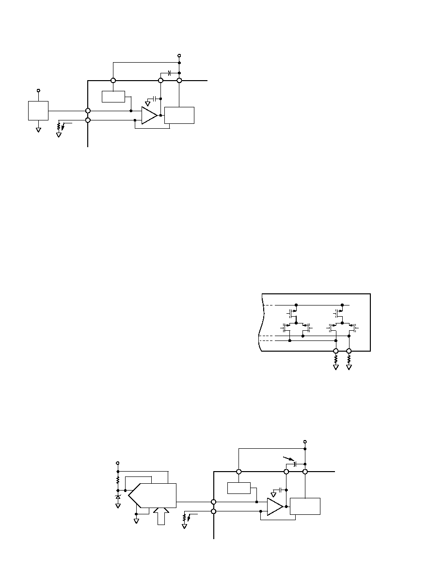
Figure 9 shows an equivalent circuit of the AD9761’s I (or Q)
DAC output. It consists of a parallel array of PMOS current
sources in which each current source is switched to either
IOUTA or IOUTB via a differential PMOS switch. As a result,
the equivalent output impedance of IOUTA and IOUTB
remains quite high (i.e., >100 k and 5 pF).
AD9761
AVDD
RLOAD
IOUTA
IOUTB
Figure 9. Equivalent Circuit of the AD9761 DAC Output
IOUTA and IOUTB have a negative and positive voltage
compliance range that must be adhered to achieve optimum
performance. The negative output compliance range of –1 V is
set by the breakdown limits of the CMOS process. Operation
beyond this maximum limit may result in a breakdown of the
output stage.
50pF
CURRENT
SOURCE
ARRAY
+1.2V REF
REFIO
FSADJ
REFLO
COMP2
AVDD
AD1580
1.2V
OPTIONAL
BAND LIMITING
CAPACITOR
IREF =
VREF/RSET
AVDD
RSET
0.1V TO 1.2V
RFB
VDD
OUT1
OUT2
AGND
VREF
AD7524
DB7–DB0
+
–
AD9761
Figure 8. Single-Supply Gain Control Circuit
REV. C
相关PDF资料 |
PDF描述 |
|---|---|
| SY88903ALKG | IC AMP POST PECL 3.3V TTL 10MSOP |
| AD7528JN | IC DAC 8BIT DUAL MULTIPLY 20-DIP |
| SY88903VKG | IC AMP POST PECL 3.3V TTL 10MSOP |
| AD7248AARZ-REEL | IC DAC 12BIT W/REF 20-SOIC |
| LTC6409CUDB#TRMPBF | IC AMP/DRIVER DIFF 10-QFN |
相关代理商/技术参数 |
参数描述 |
|---|---|
| AD9761-EB | 制造商:Analog Devices 功能描述:Evaluation Board For AD9761 制造商:Analog Devices 功能描述:DEV TOOLS, EVAL BD FOR AD9761 - Bulk 制造商:Analog Devices 功能描述:SEMICONDUCTOR ((NS)) |
| AD9761-EBZ | 功能描述:BOARD EVAL FOR AD9761 RoHS:是 类别:编程器,开发系统 >> 评估板 - 数模转换器 (DAC) 系列:TxDAC® 产品培训模块:Lead (SnPb) Finish for COTS Obsolescence Mitigation Program 标准包装:1 系列:- DAC 的数量:4 位数:12 采样率(每秒):- 数据接口:串行,SPI? 设置时间:3µs DAC 型:电流/电压 工作温度:-40°C ~ 85°C 已供物品:板 已用 IC / 零件:MAX5581 |
| AD9762 | 制造商:AD 制造商全称:Analog Devices 功能描述:Analog Devices: Data Converters: DAC 12-Bit, 10 ns to 100 ns Converters Selection Table |
| AD9762AR | 功能描述:IC DAC 12BIT 125MSPS 28-SOIC RoHS:否 类别:集成电路 (IC) >> 数据采集 - 数模转换器 系列:TxDAC® 产品培训模块:Data Converter Fundamentals DAC Architectures 标准包装:750 系列:- 设置时间:7µs 位数:16 数据接口:并联 转换器数目:1 电压电源:双 ± 功率耗散(最大):100mW 工作温度:0°C ~ 70°C 安装类型:表面贴装 封装/外壳:28-LCC(J 形引线) 供应商设备封装:28-PLCC(11.51x11.51) 包装:带卷 (TR) 输出数目和类型:1 电压,单极;1 电压,双极 采样率(每秒):143k |
发布紧急采购,3分钟左右您将得到回复。