- 您现在的位置:买卖IC网 > PDF目录10656 > AD976AANZ (Analog Devices Inc)IC ADC 16BIT 200KSPS 28-DIP PDF资料下载
参数资料
| 型号: | AD976AANZ |
| 厂商: | Analog Devices Inc |
| 文件页数: | 6/16页 |
| 文件大小: | 0K |
| 描述: | IC ADC 16BIT 200KSPS 28-DIP |
| 标准包装: | 13 |
| 位数: | 16 |
| 采样率(每秒): | 200k |
| 数据接口: | 并联 |
| 转换器数目: | 1 |
| 功率耗散(最大): | 100mW |
| 电压电源: | 模拟和数字 |
| 工作温度: | -40°C ~ 85°C |
| 安装类型: | 通孔 |
| 封装/外壳: | 28-DIP(0.600",15.24mm) |
| 供应商设备封装: | 28-PDIP |
| 包装: | 管件 |
| 输入数目和类型: | 1 个单端,双极 |
| 产品目录页面: | 777 (CN2011-ZH PDF) |
| 配用: | EVAL-AD976CB-ND - BOARD EVAL FOR AD976 EVAL-AD976ACB-ND - BOARD EVAL FOR AD976A |
AD976/AD976A
–14–
REV. C
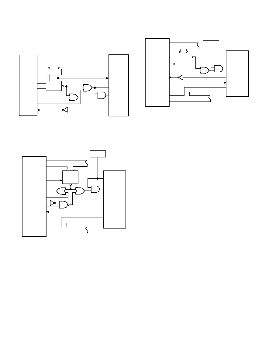
8051 Interface
Figure 21 illustrates the use of the AD976/AD976A with an
8051 microcontroller.
DB7
DB0
BYTE
A0
CS
BUS
*ADDITIONAL PINS OMITTED FOR CLARITY
BUSY
AD976/
AD976A
8051
LATCH
BUS
AD0
AD7
P0
A15
A8
P2
RD
WR
INT
R/
C
ADDR
DECODE
Figure 21. AD976/AD976A to 8051 Interface
TMS320C25 Interface
Figure 22 shows an interface between the AD976/AD976A and
the TMS320C25.
TIMER
ADDRESS BUS
*ADDITIONAL PINS OMITTED FOR CLARITY
DATA BUS
DB15
DB0
BUSY
AD976/
AD976A
R/
C
EN
ADDR
DECODE
A0
A15
D15
D0
TMS320C25
R/W
IS
READY
STRB
NSC
INT
CS
Figure 22. AD976/AD976A to TMS320C25 Interface
ADSP-2111 Interface
Figure 23 shows an interface to the ADSP-2111 signal processor.
In this example, CS is being used to control conversions and is
generated by an external timer. A conversion is initiated each
time the timer output goes low as long as you are not reading
from the AD976/AD976A and while the Flag Output (FO) pin
of the ADSP-2111 is low. When a conversion is complete, the
BUSY line will return high. With the IRQn pin programmed to
generate an interrupt on a high-to-low transition, an interrupt
will occur at the end of each conversion. The 16-bit result of the
conversion can be read from within the interrupt service routine
by first forcing FO high, then performing a read operation with
the AD976/AD976A.
ADDRESS BUS
*ADDITIONAL PINS OMITTED FOR CLARITY
DATA BUS
DB15
DB0
BUSY
AD976/
AD976A
EN
ADDR
DECODE
A0
A13
D15
D0
ADSP-2111
DMS
IRQn
CS
TIMER
RD
FO
R/
C
Figure 23. AD976/AD976A to ADSP-2111 Interface
POWER SUPPLIES AND DECOUPLING
The AD976/AD976A has two power supply input pins. VANA
and VDIG provide the supply voltages to the analog and digital
portions, respectively. VANA is the +5 V supply for the on-chip
analog circuitry, and VDIG is the +5 V supply for the on-chip
digital circuitry. The AD976/AD976A is designed to be inde-
pendent of power supply sequencing and, thus, free from supply
voltage induced latch-up.
With high performance linear circuits, changes in the power
supplies can result in undesired circuit performance. Optimally,
well regulated power supplies should be chosen with less than
1% ripple. The ac output impedance of a power supply is a
complex function of frequency and it will generally increase with
frequency. Thus, high frequency switching, such as that encoun-
tered with digital circuitry, requires the fast transient currents
that most power supplies can not adequately provide. Such a
situation results in large voltage spikes on the supplies. To com-
pensate for the finite ac output impedance of most supplies,
charge “reserves” should be stored in bypass capacitors. This
will effectively lower the supplies impedance presented to the
AD976/AD976A VANA and VDIG pins and reduce the magnitude
of these spikes. Decoupling capacitors, typically 0.1
F, should
be placed close to the power supply pins of the AD976/AD976A
to minimize any inductance between the capacitors and the
VANA and VDIG pins.
The AD976/AD976A may be operated from a single +5 V sup-
ply. When separate supplies are used, however, it is beneficial to
have larger capacitors, 10
F, placed between the logic supply
(VDIG) and digital common (DGND) and between the analog
supply (VANA) and the analog common (AGND2). Additionally,
10
F capacitors should be located in the vicinity of the ADC to
further reduce low frequency ripple. In systems where the device
will be subjected to harsh environmental noise, additional de-
coupling may be required.
相关PDF资料 |
PDF描述 |
|---|---|
| MAX982CPA+ | IC COMPARATOR OD 8-DIP |
| AD7674ASTZ | IC ADC 18BIT 800KSPS 48-LQFP |
| AD7984BRMZ | IC ADC 18BIT 1.3MSPS SAR 10MSOP |
| MAX9040AEUK+T | IC COMPARATOR SNGL SOT23-5 |
| AD7671ASTZ | IC ADC 16BIT CMOS 1MSPS 48-LQFP |
相关代理商/技术参数 |
参数描述 |
|---|---|
| AD976AANZ | 制造商:Analog Devices 功能描述:IC 16-BIT ADC |
| AD976AAR | 功能描述:IC ADC 16BIT 200KSPS 28-SOIC RoHS:否 类别:集成电路 (IC) >> 数据采集 - 模数转换器 系列:- 标准包装:1 系列:- 位数:14 采样率(每秒):83k 数据接口:串行,并联 转换器数目:1 功率耗散(最大):95mW 电压电源:双 ± 工作温度:0°C ~ 70°C 安装类型:通孔 封装/外壳:28-DIP(0.600",15.24mm) 供应商设备封装:28-PDIP 包装:管件 输入数目和类型:1 个单端,双极 |
| AD976AARS | 功能描述:IC ADC 16BIT 200KSPS 28-SSOP RoHS:否 类别:集成电路 (IC) >> 数据采集 - 模数转换器 系列:- 标准包装:1 系列:- 位数:14 采样率(每秒):83k 数据接口:串行,并联 转换器数目:1 功率耗散(最大):95mW 电压电源:双 ± 工作温度:0°C ~ 70°C 安装类型:通孔 封装/外壳:28-DIP(0.600",15.24mm) 供应商设备封装:28-PDIP 包装:管件 输入数目和类型:1 个单端,双极 |
| AD976AARSRL | 制造商:Analog Devices 功能描述:ADC Single SAR 200ksps 16-bit Parallel 28-Pin SSOP T/R |
| AD976AARSZ | 功能描述:IC ADC 16BIT 200KSPS 28SSOP RoHS:是 类别:集成电路 (IC) >> 数据采集 - 模数转换器 系列:- 其它有关文件:TSA1204 View All Specifications 标准包装:1 系列:- 位数:12 采样率(每秒):20M 数据接口:并联 转换器数目:2 功率耗散(最大):155mW 电压电源:模拟和数字 工作温度:-40°C ~ 85°C 安装类型:表面贴装 封装/外壳:48-TQFP 供应商设备封装:48-TQFP(7x7) 包装:Digi-Reel® 输入数目和类型:4 个单端,单极;2 个差分,单极 产品目录页面:1156 (CN2011-ZH PDF) 其它名称:497-5435-6 |
发布紧急采购,3分钟左右您将得到回复。