参数资料
| 型号: | AD977ABNZ |
| 厂商: | Analog Devices Inc |
| 文件页数: | 24/24页 |
| 文件大小: | 0K |
| 描述: | IC ADC 16BIT 200KSPS 20DIP |
| 产品变化通告: | Product Discontinuance 27/Oct/2011 |
| 标准包装: | 1 |
| 位数: | 16 |
| 采样率(每秒): | 200k |
| 数据接口: | 串行,SPI? |
| 转换器数目: | 1 |
| 功率耗散(最大): | 100mW |
| 电压电源: | 模拟和数字 |
| 工作温度: | -40°C ~ 85°C |
| 安装类型: | 通孔 |
| 封装/外壳: | 20-DIP(0.300",7.62mm) |
| 供应商设备封装: | 20-PDIP |
| 包装: | 管件 |
| 输入数目和类型: | 3 个单端,单极;3 个单端,双极 |
| 配用: | EVAL-AD977CB-ND - BOARD EVAL FOR AD977 EVAL-AD977ACB-ND - BOARD EVAL FOR AD977A |
AD977/AD977A
–9–
REV. D
normally low or normally high when inactive. In the case of the
discontinuous clock, the AD977/AD977A can be configured to
either generate or not generate a SYNC output (with a continu-
ous clock a SYNC output will always be produced).
Each of the methods will be described in the following sections
and are illustrated in Figures 4 through 9. It should be noted
that all timing diagrams assume that the receiving device is
latching data on the rising edge of the external clock. If the
falling edge of DATACLK is used then, in the case of a discon-
tinuous clock, one less clock pulse is required than shown in
Figures 4 through 7 to latch in a 16-bit word. Note that data is
valid on the falling edge of a clock pulse (for t13 greater than t18)
and the rising edge of the next clock pulse.
The AD977 provides error correction circuitry that can correct
for an improper bit decision made during the first half of the
conversion cycle. Normally the occurrence of an incorrect bit
decision during a conversion cycle is irreversible. This error
occurs as a result of noise during the time of the decision or due
to insufficient settling time. As the AD977/AD977A is perform-
ing a conversion it is important that transitions not occur on
digital input/output pins or degradation of the conversion result
could occur. This is particularly important during the second
half of the conversion process. For this reason it is recommended
that when an external clock is being provided it be a discontinu-
ous clock that is not toggling during the time that
BUSY is low
or, more importantly, that it does not transition during the latter
half of
BUSY low.
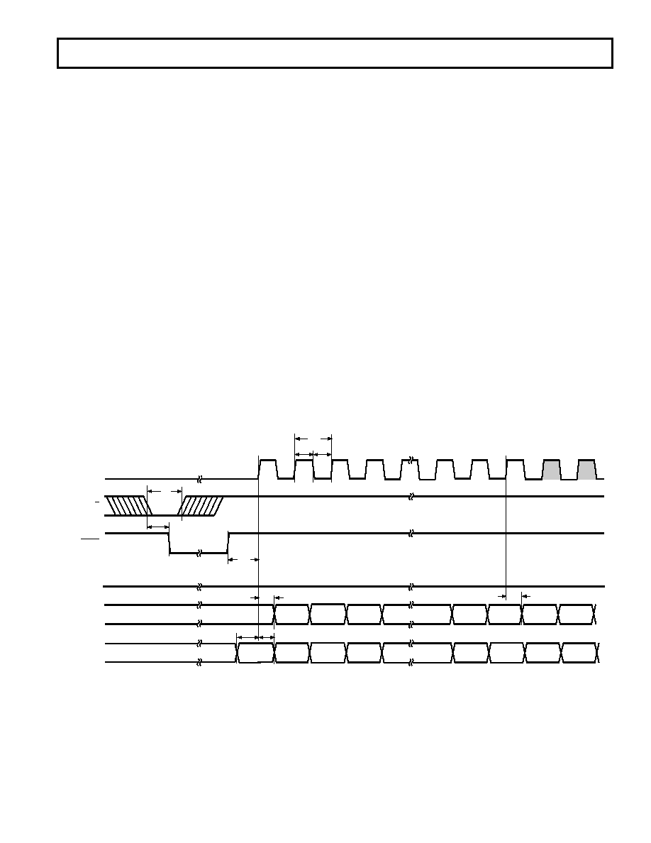
EXTERNAL DISCONTINUOUS CLOCK DATA READ
AFTER CONVERSION NO SYNC OUTPUT GENERATED
Figure 4 illustrates the method by which data from conversion
“n” can be read after the conversion is complete using a discon-
tinuous external clock without the generation of a SYNC
output. After a conversion is complete, indicated by
BUSY
returning high, the result of that conversion can be read while
CS is Low and R/C is high. In this mode CS can be tied low.
The MSB will be valid on the first falling edge and the second
rising edge of DATACLK. The LSB will be valid on the 16th
falling edge and the 17th rising edge of DATACLK. A mini-
mum of 16 clock pulses are required for DATACLK if the
receiving device will be latching data on the falling edge of
DATACLK. A minimum of 17 clock pulses are required for
DATACLK if the receiving device will be latching data on the
rising edge of DATACLK. Approximately 40 ns after the 17th
rising edge of DATACLK (if provided) the DATA output pin
will reflect the state of the TAG input pin during the first rising
edge of DATACLK.
The advantage of this method of reading data is that it is not
being clocked out during a conversion and therefore conversion
performance is not degraded.
When reading data after the conversion is complete, with the
highest frequency permitted for DATACLK (15.15 MHz), and
with the AD977A, the maximum possible throughput is approxi-
mately 195 kHz and not the rated 200 kHz.
For details on use of the TAG input with this mode see the Use
of the Tag Feature section.
BUSY
R/C
EXT
DATACLK
t13
t18
BIT 15
(MSB)
BIT 14
12
DATA
SYNC
t14
t12
0
3
14
15
16
t1
t2
t24
t21
BIT 13
BIT 1
BIT 0
(LSB)
TAG 0
TAG 1
t23
TAG 0
TAG 1
TAG 2
TAG 3
TAG 15
TAG 16
TAG 17
t18
TAG 18
TAG
Figure 4. Conversion and Read Timing Using an External Discontinuous Data Clock (EXT/
INT Set to Logic High, CS Set
to Logic Low)
相关PDF资料 |
PDF描述 |
|---|---|
| AD9781BCPZ | IC DAC 14BT 500MSPS LVDS 72LFCSP |
| AD9877ABSZ | IC PROCESSOR FRONT END 100MQFP |
| AD9878BSTZ | IC FRONT-END MIXED-SGNL 100-LQFP |
| AD9879BSZ | IC PROCESSOR FRONT END 100MQFP |
| AD9901KQ | IC PHASE/FREQ DISCRIMR 14-CDIP |
相关代理商/技术参数 |
参数描述 |
|---|---|
| AD977ABR | 功能描述:IC ADC 16BIT 200KSPS 20-SOIC RoHS:否 类别:集成电路 (IC) >> 数据采集 - 模数转换器 系列:- 标准包装:1 系列:- 位数:14 采样率(每秒):83k 数据接口:串行,并联 转换器数目:1 功率耗散(最大):95mW 电压电源:双 ± 工作温度:0°C ~ 70°C 安装类型:通孔 封装/外壳:28-DIP(0.600",15.24mm) 供应商设备封装:28-PDIP 包装:管件 输入数目和类型:1 个单端,双极 |
| AD977ABRS | 功能描述:IC ADC 16BIT 200KSPS 28-SSOP RoHS:否 类别:集成电路 (IC) >> 数据采集 - 模数转换器 系列:- 标准包装:1 系列:- 位数:14 采样率(每秒):83k 数据接口:串行,并联 转换器数目:1 功率耗散(最大):95mW 电压电源:双 ± 工作温度:0°C ~ 70°C 安装类型:通孔 封装/外壳:28-DIP(0.600",15.24mm) 供应商设备封装:28-PDIP 包装:管件 输入数目和类型:1 个单端,双极 |
| AD977ABRSRL | 制造商:Analog Devices 功能描述:ADC Single SAR 200ksps 16-bit Serial 28-Pin SSOP T/R 制造商:Analog Devices 功能描述:ADC SGL SAR 200KSPS 16BIT SERL 28SSOP - Tape and Reel 制造商:Rochester Electronics LLC 功能描述:200 KSPS 16 BIT ADC - Tape and Reel |
| AD977ABRSZ | 功能描述:IC ADC 16BIT 200KSPS 28-SSOP RoHS:是 类别:集成电路 (IC) >> 数据采集 - 模数转换器 系列:- 其它有关文件:TSA1204 View All Specifications 标准包装:1 系列:- 位数:12 采样率(每秒):20M 数据接口:并联 转换器数目:2 功率耗散(最大):155mW 电压电源:模拟和数字 工作温度:-40°C ~ 85°C 安装类型:表面贴装 封装/外壳:48-TQFP 供应商设备封装:48-TQFP(7x7) 包装:Digi-Reel® 输入数目和类型:4 个单端,单极;2 个差分,单极 产品目录页面:1156 (CN2011-ZH PDF) 其它名称:497-5435-6 |
| AD977ABRSZRL | 功能描述:IC ADC 16BIT 200KSPS 28SSOP RoHS:是 类别:集成电路 (IC) >> 数据采集 - 模数转换器 系列:- 标准包装:1 系列:- 位数:14 采样率(每秒):83k 数据接口:串行,并联 转换器数目:1 功率耗散(最大):95mW 电压电源:双 ± 工作温度:0°C ~ 70°C 安装类型:通孔 封装/外壳:28-DIP(0.600",15.24mm) 供应商设备封装:28-PDIP 包装:管件 输入数目和类型:1 个单端,双极 |
发布紧急采购,3分钟左右您将得到回复。