- 您现在的位置:买卖IC网 > PDF目录17059 > AD9783-DPG2-EBZ (Analog Devices Inc)BOARD EVAL FOR AD9783 PDF资料下载
参数资料
| 型号: | AD9783-DPG2-EBZ |
| 厂商: | Analog Devices Inc |
| 文件页数: | 30/32页 |
| 文件大小: | 0K |
| 描述: | BOARD EVAL FOR AD9783 |
| 标准包装: | 1 |
| 系列: | * |
第1页第2页第3页第4页第5页第6页第7页第8页第9页第10页第11页第12页第13页第14页第15页第16页第17页第18页第19页第20页第21页第22页第23页第24页第25页第26页第27页第28页第29页当前第30页第31页第32页
Data Sheet
AD9780/AD9781/AD9783
Rev. B | Page 7 of 32
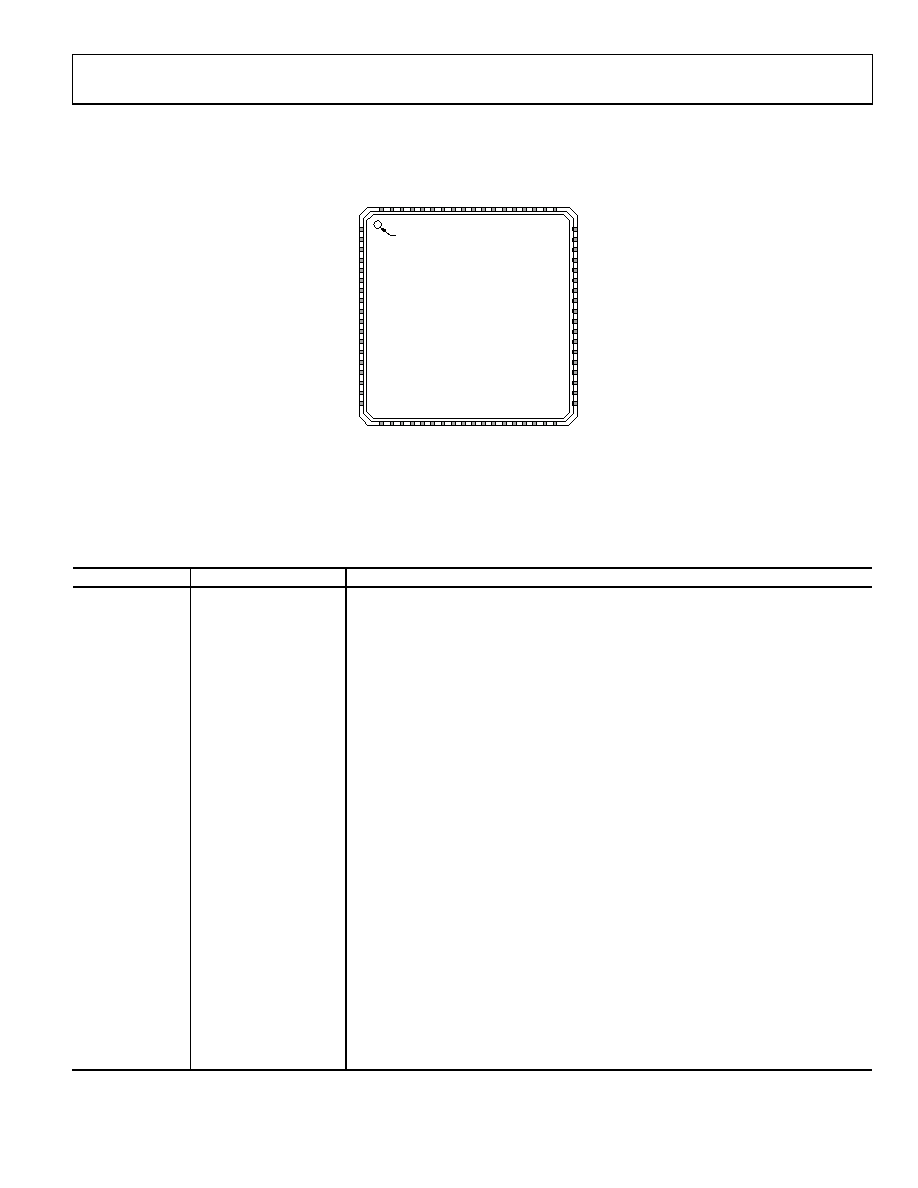
PIN CONFIGURATIONS AND FUNCTION DESCRIPTIONS
06936-
002
1
2
3
4
5
6
7
8
9
10
11
12
13
14
15
16
CVDD18
CVSS
CLKP
CLKN
CVSS
CVDD18
DVSS
DVDD18
D11P
D11N
D10P
D10N
D9P
D9N
D8P
D8N
17
D7P
18
D7N
19
20
21
22
23
24
25
26
27
28
29
30
31
32
33
34
D6
P
D6N
D5
P
D5N
D4
P
D4N
DCO
P
DCO
N
DV
DD33
D
VSS
DCI
P
DCI
N
D3
P
D3N
D2
P
D2N
35
D1
P
36
D1N
54
53
52
51
50
49
48
47
46
45
44
43
42
41
40
39
38
37
FS ADJ
RESET
CSB
SCLK
SDIO
SDO
DVSS
DVDD18
NC
D0N
D0P
72
71
70
69
68
67
66
65
64
63
62
61
60
59
58
57
56
55
A
V
DD33
A
V
DD33
A
VSS
IOU
T1
P
IOU
T1
N
A
VSS
AUX
1
P
AUX
1N
A
VSS
AUX
2N
AUX
2
P
A
VSS
IOU
T2
N
IOU
T2
P
A
VSS
A
V
DD33
A
V
DD33
R
E
FIO
NOTES
1. NC = NO CONNECT
2. EXPOSED PAD MUST BE
SOLDERED TO PCB AND
CONNECTED TO AVSS.
PIN 1
INDICATOR
AD9780
(TOP VIEW)
Figure 2. AD9780 Pin Configuration
Table 6. AD9780 Pin Function Descriptions
Pin No.
Mnemonic
Description
1, 6
CVDD18
Clock Supply Voltage (1.8 V).
2, 5
CVSS
Clock Supply Return.
3, 4
CLKP, CLKN
Differential DAC Sampling Clock Input.
7, 28, 48
DVSS
Digital Common.
8, 47
DVDD18
Digital Supply Voltage (1.8 V).
9 to 24, 31 to 38
D11P, D11N to D0P, D0N
LVDS Data Inputs. D11 is the MSB, D0 is the LSB.
25, 26
DCOP, DCON
Differential Data Clock Output. Clock at the DAC sample rate.
27
DVDD33
Digital Input and Output Pad Ring Supply Voltage (3.3 V).
29, 30
DCIP, DCIN
Differential Data Clock Input. Clock aligned with input data.
39 to 46
NC
No Connection. Leave these pins floating.
49
SDO
Serial Port Data Output.
50
SDIO
Serial Port Data Input (4-Wire Mode) or Bidirectional Serial Data Line (3-Wire Mode).
51
SCLK
Serial Port Clock Input.
52
CSB
Serial Port Chip Select (Active Low).
53
RESET
Chip Reset (Active High).
54
FS ADJ
Full-Scale Current Output Adjust.
55
REFIO
Analog Reference Input/Output (1.2 V Nominal).
56, 57, 71, 72
AVDD33
Analog Supply Voltage (3.3 V).
58, 61, 64, 67, 70
AVSS
Analog Common.
59
IOUT2P
DAC Current Output. Full-scale current is sourced when all data bits are 1s.
60
IOUT2N
Complementary DAC Current Output. Full-scale current is sourced when all data bits are 0s.
62, 63
AUX2P, AUX2N
Differential Auxiliary DAC Current Output (Channel 2).
65, 66
AUX1N, AUX1P
Differential Auxiliary DAC Current Output (Channel 1).
68
IOUT1N
Complementary DAC Current Output. Full-scale current is sourced when all data bits are 0s.
69
IOUT1P
DAC Current Output. Full-scale current is sourced when all data bits are 1s.
Heat Sink Pad
N/A
The heat sink pad on the bottom of the package should be soldered to the PCB plane that
carries AVSS.
相关PDF资料 |
PDF描述 |
|---|---|
| AD9707-DPG2-EBZ | BOARD EVAL FOR AD9707 |
| AD9704-DPG2-EBZ | BOARD EVAL FOR AD9704 |
| AD9741-DPG2-EBZ | IC DAC DUAL 8BIT 200MSPS 72LFCSP |
| 0210490186 | CABLE JUMPER 1.25MM .254M 12POS |
| AD9743-DPG2-EBZ | IC DAC DUAL 10BIT 72LFCSP |
相关代理商/技术参数 |
参数描述 |
|---|---|
| AD9783-DUAL-EBZ | 制造商:Analog Devices 功能描述:DUAL 16B, 500 MSPS LVDS DAC - Boxed Product (Development Kits) |
| AD9783-EBZ | 制造商:Analog Devices 功能描述:DUAL 16B, 600 MSPS LVDS DAC - Bulk |
| AD9784 | 制造商:AD 制造商全称:Analog Devices 功能描述:14-Bit, 200 MSPS/500 MSPS TxDAC+ with 2×/4×/8× Interpolation and Signal Processing |
| AD9785 | 制造商:AD 制造商全称:Analog Devices 功能描述:Dual 12-/14-/16-Bit 800 MSPS DAC with Low Power 32-Bit Complex NCO |
| AD9785BSVZ | 功能描述:IC DAC 12BIT 800MSPS 100TQFP RoHS:是 类别:集成电路 (IC) >> 数据采集 - 数模转换器 系列:TxDAC® 标准包装:1 系列:- 设置时间:4.5µs 位数:12 数据接口:串行,SPI? 转换器数目:1 电压电源:单电源 功率耗散(最大):- 工作温度:-40°C ~ 125°C 安装类型:表面贴装 封装/外壳:8-SOIC(0.154",3.90mm 宽) 供应商设备封装:8-SOICN 包装:剪切带 (CT) 输出数目和类型:1 电压,单极;1 电压,双极 采样率(每秒):* 其它名称:MCP4921T-E/SNCTMCP4921T-E/SNRCTMCP4921T-E/SNRCT-ND |
发布紧急采购,3分钟左右您将得到回复。