参数资料
| 型号: | AD9783BCPZ |
| 厂商: | Analog Devices Inc |
| 文件页数: | 22/32页 |
| 文件大小: | 0K |
| 描述: | IC DAC 16BT 500MSPS LVDS 72LFCSP |
| 产品培训模块: | Data Converter Fundamentals DAC Architectures |
| 标准包装: | 1 |
| 位数: | 16 |
| 数据接口: | 串行 |
| 转换器数目: | 2 |
| 电压电源: | 模拟和数字 |
| 功率耗散(最大): | 315mW |
| 工作温度: | -40°C ~ 85°C |
| 安装类型: | 表面贴装 |
| 封装/外壳: | 72-VFQFN 裸露焊盘,CSP |
| 供应商设备封装: | 72-LFCSP-VQ(10x10) |
| 包装: | 托盘 |
| 输出数目和类型: | 4 电流,单极;4 电流,双极 |
| 采样率(每秒): | 600M |
第1页第2页第3页第4页第5页第6页第7页第8页第9页第10页第11页第12页第13页第14页第15页第16页第17页第18页第19页第20页第21页当前第22页第23页第24页第25页第26页第27页第28页第29页第30页第31页第32页
Data Sheet
AD9780/AD9781/AD9783
Rev. B | Page 29 of 32
In return-to-zero mode, the output is set to midscale every
other half clock cycle. The output is similar to the DAC output
in normal mode except that the output pulses are half the width
and half the area. Because the output pulses have half the width,
the sinc function is scaled in frequency by two and has a first
null at 2 × fDAC. Because the area of the pulses is half that of the
pulses in normal mode, the output power is half the normal
mode output power.
06936-
061
D9
D8
D7
D6
D5
D4
D3
D2
D1
D10
INPUT DATA
DAC CLK
QUAD-SWITCH
DAC OUTPUT
(
fS MIX MODE)
QUAD-SWITCH
DAC OUTPUT
(RETURN-TO-
ZERO MODE)
t
Figure 64. Mix Mode and Return-to-Zero Mode DAC Waveforms
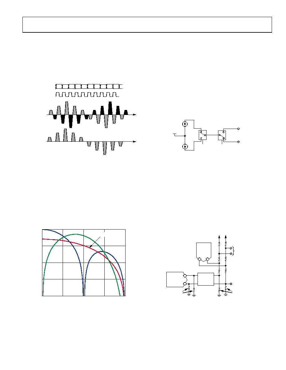
The functions that shape the output spectrums for the three
modes of operation, normal mode, mix mode, and return-to-
zero mode, are shown in Figure 65. Switching between the
analog modes reshapes the sinc roll-off inherent at the DAC
output. This ability to change modes in the AD9780/AD9781/
AD9783 makes the parts suitable for direct IF applications. The
user can place a carrier anywhere in the first three Nyquist
zones depending on the operating mode selected. The perfor-
mance and maximum amplitude in all three Nyquist zones is
impacted by this sinc roll-off depending on where the carrier is
placed, as shown in Figure 65.
06936-
062
0
–10
–20
–30
–40
T
(f)
(d
B
)
0.5
0
1.5
1.0
2.0
(
fS)
NORMAL
MIX
RETURN-TO-ZERO
Figure 65. Transfer Function for Each Analog Operating Mode
Auxiliary DACs
Two auxiliary DACs are provided on the AD9780/AD9781/
AD9783. A functional diagram is shown in Figure 66. The
auxiliary DACs are current output devices with two output
pins, AUXP and AUXN. The active pin can be programmed to
either source or sink current. When either sinking or sourcing,
the full-scale current magnitude is 2 mA. The available compliance
range at the auxiliary DAC outputs depends on whether the output
is configured to sink or source current. When sourcing current,
the compliance voltage is 0 V to 1.6 V, but when sinking current,
the output compliance voltage is reduced to 0.8 V to 1.6 V. Either
output can be used, but only one output of the AUX DAC (P or
N) is active at any time. The inactive pin is always in a high
impedance state (>100 kΩ).
06936-
063
VBIAS
AUXP
AUXN
SINK
OR
SOURCE
POSITIVE
OR
NEGATIVE
0mA
TO
2mA
0mA
TO
2mA
Figure 66. Auxiliary DAC Functional Diagram
In a single sideband transmitter application, the combination of
the input referred dc offset voltage of the quadrature modulator
and the DAC output offset voltage can result in local oscillator
(LO) feedthrough at the modulator output, which degrades system
performance. The auxiliary DACs can be used to remove the dc
offset and the resulting LO feedthrough. The circuit configura-
tion for using the auxiliary DACs for performing dc offset
correction depends on the details of the DAC and modulator
interface. An example of a dc-coupled configuration with low-
pass filtering is shown in Figure 67.
AD9783
AUX
DAC1 OR
DAC2
AD9783
DAC1 OR
DAC2
25 TO 50
QUAD MOD
I OR Q INPUTS
QUADRATURE
MODULATOR V+
25 TO 50
06936-
064
OPTIONAL
PASSIVE
FILTERING
Figure 67. DAC DC-Coupled to Quadrature Modulator with a Passive DC Shift
相关PDF资料 |
PDF描述 |
|---|---|
| MS3121F22-41P | CONN RCPT 41POS CBL MNT W/PINS |
| ICS843202AYILFT | IC SYNTHESIZER 680MHZ 32-LQFP |
| MS3450W20-2S | CONN RCPT 1POS WALL MNT W/SCKT |
| VE-J4N-MZ-F1 | CONVERTER MOD DC/DC 18.5V 25W |
| VI-2ND-MW-F4 | CONVERTER MOD DC/DC 85V 100W |
相关代理商/技术参数 |
参数描述 |
|---|---|
| AD9783BCPZRL | 功能描述:IC DAC 16BT 500MSPS LVDS 72LFCSP RoHS:是 类别:集成电路 (IC) >> 数据采集 - 数模转换器 系列:- 产品培训模块:Data Converter Fundamentals DAC Architectures 标准包装:750 系列:- 设置时间:7µs 位数:16 数据接口:并联 转换器数目:1 电压电源:双 ± 功率耗散(最大):100mW 工作温度:0°C ~ 70°C 安装类型:表面贴装 封装/外壳:28-LCC(J 形引线) 供应商设备封装:28-PLCC(11.51x11.51) 包装:带卷 (TR) 输出数目和类型:1 电压,单极;1 电压,双极 采样率(每秒):143k |
| AD9783-DPG2-EBZ | 功能描述:BOARD EVAL FOR AD9783 RoHS:是 类别:编程器,开发系统 >> 评估板 - 数模转换器 (DAC) 系列:* 产品培训模块:Lead (SnPb) Finish for COTS Obsolescence Mitigation Program 标准包装:1 系列:- DAC 的数量:4 位数:12 采样率(每秒):- 数据接口:串行,SPI? 设置时间:3µs DAC 型:电流/电压 工作温度:-40°C ~ 85°C 已供物品:板 已用 IC / 零件:MAX5581 |
| AD9783-DUAL-EBZ | 制造商:Analog Devices 功能描述:DUAL 16B, 500 MSPS LVDS DAC - Boxed Product (Development Kits) |
| AD9783-EBZ | 制造商:Analog Devices 功能描述:DUAL 16B, 600 MSPS LVDS DAC - Bulk |
| AD9784 | 制造商:AD 制造商全称:Analog Devices 功能描述:14-Bit, 200 MSPS/500 MSPS TxDAC+ with 2×/4×/8× Interpolation and Signal Processing |
发布紧急采购,3分钟左右您将得到回复。