- 您现在的位置:买卖IC网 > PDF目录11656 > AD9814JRRL (Analog Devices Inc)IC CCD SIGNAL PROC 14BIT 28-SOIC PDF资料下载
参数资料
| 型号: | AD9814JRRL |
| 厂商: | Analog Devices Inc |
| 文件页数: | 9/15页 |
| 文件大小: | 0K |
| 描述: | IC CCD SIGNAL PROC 14BIT 28-SOIC |
| 标准包装: | 1,000 |
| 类型: | CCD 信号处理器,14 位 |
| 输入类型: | 逻辑 |
| 输出类型: | 逻辑 |
| 接口: | 3 线串口 |
| 电流 - 电源: | 80mA |
| 安装类型: | 表面贴装 |
| 封装/外壳: | 28-SOIC(0.295",7.50mm 宽) |
| 供应商设备封装: | 28-SOIC W |
| 包装: | 带卷 (TR) |
REV. 0
–3–
AD9814
DIGITAL SPECIFICATIONS
Parameter
Symbol
Min
Typ
Max
Units
LOGIC INPUTS
High Level Input Voltage
VIH
2.6
V
Low Level Input Voltage
VIL
0.8
V
High Level Input Current
IIH
10
A
Low Level Input Current
IIL
10
A
Input Capacitance
CIN
10
pF
LOGIC OUTPUTS
High Level Output Voltage
VOH
4.5
V
Low Level Output Voltage
VOL
0.1
V
High Level Output Current
IOH
50
A
Low Level Output Current
IOL
50
A
Specifications subject to change without notice.
TIMING SPECIFICATIONS
Parameter
Symbol
Min
Typ
Max
Units
CLOCK PARAMETERS
3-Channel Pixel Rate
tPRA
300
500
ns
1-Channel Pixel Rate
tPRB
140
ns
ADCCLK Pulsewidth
tADCLK
45
ns
CDSCLK1 Pulsewidth
tC1
20
ns
CDSCLK2 Pulsewidth
tC2
40
ns
CDSCLK1 Falling to CDSCLK2 Rising
tC1C2
0ns
ADCCLK Falling to CDSCLK2 Rising
tADC2
10
ns
CDSCLK2 Rising to ADCCLK Rising
tC2ADR
10
ns
CDSCLK2 Falling to ADCCLK Falling
tC2ADF
50
ns
CDSCLK2 Falling to CDSCLK1 Rising
tC2C1
50
ns
ADCCLK Falling to CDSCLK1 Rising
tADC1
0ns
Aperture Delay for CDS Clocks
tAD
3ns
SERIAL INTERFACE
Maximum SCLK Frequency
fSCLK
10
MHz
SLOAD to SCLK Set-Up Time
tLS
10
ns
SCLK to SLOAD Hold Time
tLH
10
ns
SDATA to SCLK Rising Set-Up Time
tDS
10
ns
SCLK Rising to SDATA Hold Time
tDH
10
ns
SCLK Falling to SDATA Valid
tRDV
10
ns
DATA OUTPUT
Output Delay
tOD
6ns
3-State to Data Valid
tDV
16
ns
Output Enable High to 3-State
tHZ
5ns
Latency (Pipeline Delay)
3 (Fixed)
Cycles
Specifications subject to change without notice.
(TMIN to TMAX, AVDD = +5 V, DRVDD = +5 V, CDS Mode, fADCCLK = 6 MHz, fCDSCLK1 = fCDSCLK2 = 2 MHz,
CL = 10 pF, unless otherwise noted.)
(TMIN to TMAX, AVDD = +5 V, DRVDD = +5 V)
NOTES
1The Integral Nonlinearity in measured using the “fixed endpoint” method, NOT using a “best-fit” calculation. See Definitions of Specifications.
2The Gain Error specification is dominated by the tolerance of the internal differential voltage reference.
3Linear input signal range is from 0 V to 4 V when the CCD’s reference level is clamped to 4 V by the AD9814’s input clamp. A larger reset transient can be tolerated
by using the 3 V clamp level instead of the nominal 4 V clamp level. Linear input signal range will be from 0 V to 3 V when using the 3 V clamp level.
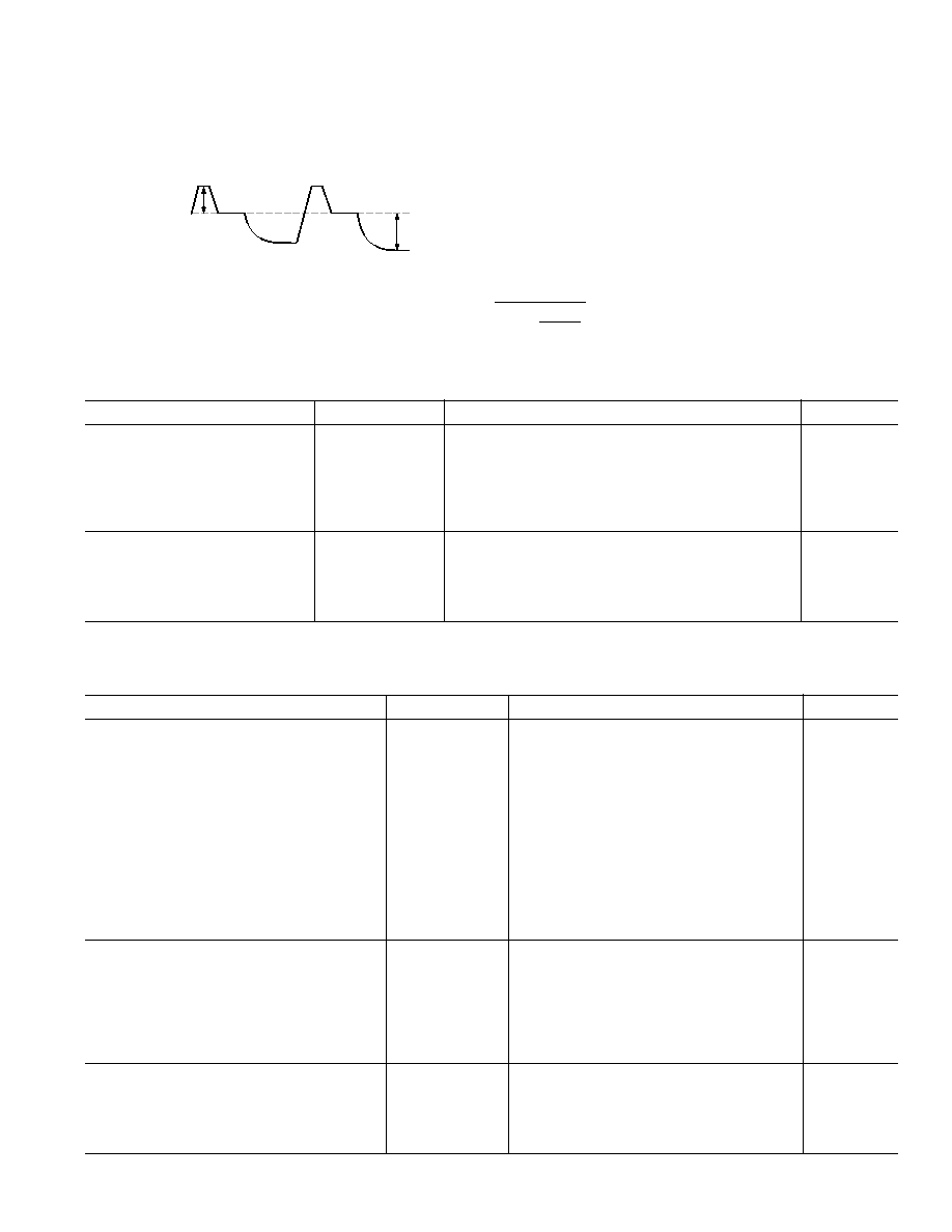
1V TYP
RESET TRANSIENT
4V SET BY INPUT CLAMP (3V OPTION ALSO AVAILABLE)
4V p-p MAX INPUT SIGNAL RANGE
GND
4The input limits are defined as the maximum tolerable voltage levels into the AD9814. These levels are not intended to be in the linear input range of the device.
Signals beyond the input limits will turn on the overvoltage protection diodes.
5The PGA Gain is approximately “linear in dB” and follows the equation: Gain
=
+
[
.
.[
]
58
14 8
63 –G
63
where G is the register value. See Figure 13.
Specifications subject to change without notice.
相关PDF资料 |
PDF描述 |
|---|---|
| D38999/26JF32SC | CONN PLUG 32POS STRAIGHT W/SCKT |
| CS3100A-24-58S | CONN RCPT 13POS WALL MNT W/SCKT |
| MCR908JK3ECPE | IC MCU FLASH 8BIT RC OSC 20-DIP |
| MS3110P22-21S | CONN RCPT 21POS WALL MNT W/SCKT |
| MC9S08EL16CTJ | MCU 16KB FLASH SLIC 20TSSOP |
相关代理商/技术参数 |
参数描述 |
|---|---|
| AD9814KR | 制造商:Analog Devices 功能描述:AFE Video 1ADC 14-Bit 5V 28-Pin SOIC W 制造商:Analog Devices 功能描述:14 BIT 6 MSPS SCANNER ANALOG FRONT END - Rail/Tube 制造商:Rochester Electronics LLC 功能描述:14 BIT 6 MSPS SCANNER ANALOG FRONT END - Bulk |
| AD9814KRRL | 制造商:Analog Devices 功能描述:AFE Video 1ADC 14-Bit 5V 28-Pin SOIC W 制造商:Analog Devices 功能描述:14 BIT 6 MSPS SCANNER ANALOG FRONT END - Tape and Reel 制造商:Rochester Electronics LLC 功能描述:14 BIT 6 MSPS SCANNER ANALOG FRONT END - Bulk |
| AD9814S | 制造商:AD 制造商全称:Analog Devices 功能描述:14-Bit CCD/CIS Signal Processor |
| AD9816 | 制造商:AD 制造商全称:Analog Devices 功能描述:Complete 12-Bit 6 MSPS CCD/CIS Signal Processor |
| AD9816-EB | 制造商:Analog Devices 功能描述:12-BIT 4MSPS CCD/CIS SIGNAL PROCESSOR - Bulk |
发布紧急采购,3分钟左右您将得到回复。