- 您现在的位置:买卖IC网 > PDF目录10979 > AD9830ASTZ (Analog Devices Inc)IC DDS 10BIT 50MHZ CMOS 48-TQFP PDF资料下载
参数资料
| 型号: | AD9830ASTZ |
| 厂商: | Analog Devices Inc |
| 文件页数: | 3/16页 |
| 文件大小: | 0K |
| 描述: | IC DDS 10BIT 50MHZ CMOS 48-TQFP |
| 产品培训模块: | Direct Digital Synthesis Tutorial Series (1 of 7): Introduction Direct Digital Synthesizer Tutorial Series (7 of 7): DDS in Action Direct Digital Synthesis Tutorial Series (3 of 7): Angle to Amplitude Converter Direct Digital Synthesis Tutorial Series (6 of 7): SINC Envelope Correction Direct Digital Synthesis Tutorial Series (4 of 7): Digital-to-Analog Converter Direct Digital Synthesis Tutorial Series (2 of 7): The Accumulator |
| 标准包装: | 1 |
| 分辨率(位): | 10 b |
| 主 fclk: | 50MHz |
| 调节字宽(位): | 32 b |
| 电源电压: | 4.75 V ~ 5.25 V |
| 工作温度: | -40°C ~ 85°C |
| 安装类型: | 表面贴装 |
| 封装/外壳: | 48-LQFP |
| 供应商设备封装: | 48-LQFP(7x7) |
| 包装: | 托盘 |
| 产品目录页面: | 552 (CN2011-ZH PDF) |
| 配用: | EVAL-AD9830EBZ-ND - BOARD EVALUATION AD9830 |
AD9830
–11–
full-scale voltage developed across it does not exceed the voltage
compliance range. Since full-scale current is controlled by RSET,
adjustments to RSET can balance changes made to the load resistor.
However, if the DAC full-scale output current is significantly less
than 20 mA, the linearity of the DAC may degrade.
DSP and MPU Interfacing
The AD9830 has a parallel interface, with 16 bits of data being
loaded during each write cycle.
The frequency or phase registers are loaded by asserting the WR
signal. The destination register for the 16-bit data is selected
using the address inputs A0, A1 and A2. The phase registers
are 12 bits wide so, only the 12 LSBs need to be valid—the
4 MSBs of the 16 bit word do not have to contain valid data.
Data is loaded into the AD9830 by pulsing WR low, the data
being latched into the AD9830 on the rising edge of WR. The
values of inputs A0, A1 and A2 are also latched into the
AD9830 on the WR rising edge. The appropriate register is up-
dated on the next MCLK rising edge. To ensure that the
AD9830 contains valid data at the rising edge of MCLK, the
rising edge of the WR pulse should not coincide with the rising
MCLK edge. The WR pulse must occur several nanoseconds
before the MCLK rising edge. If the WR rising edge occurs at
the MCLK rising edge, there is an uncertainty of one MCLK
cycle regarding the loading of the destination register—the desti-
nation register may be loaded with the new data immediately or
the destination register may be updated on the next MCLK ris-
ing edge. To avoid any uncertainty, the times listed in the speci-
fications should be complied with.
FSELECT, PSEL0 and PSEL1 are sampled on the MCLK
rising edge. Again, these inputs should be valid when an
MCLK rising edge occurs as there will be an uncertainty of one
MCLK cycle introduced otherwise. When these inputs change
value, there will be a pipeline delay before control is transferred
to the selected register—there will be a pipeline delay before the
analog output is controlled by the selected register. Similarly,
there is a delay when a new word is written to a register. PSEL0,
PSEL1, FSELECT and WR have latencies of six MCLK cycles.
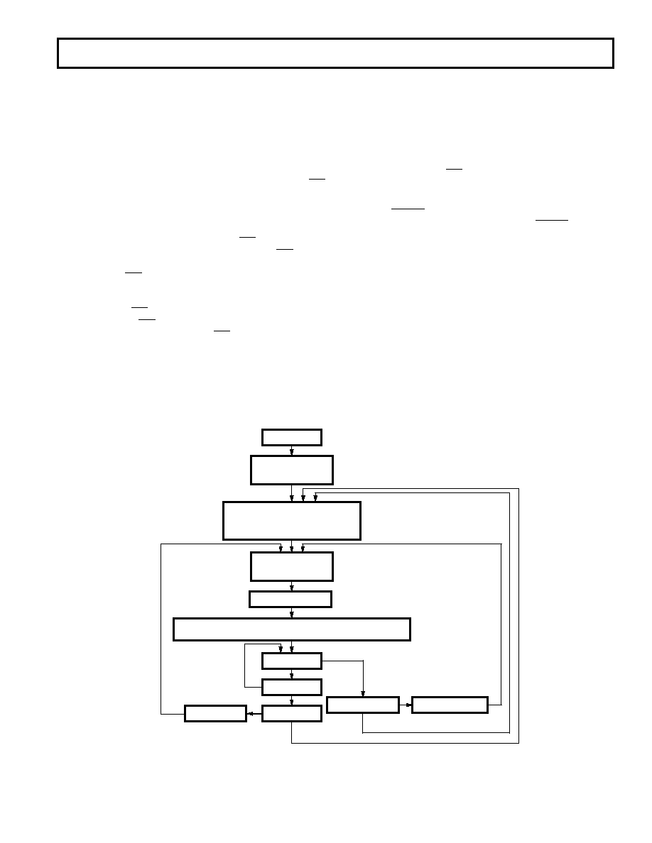
The flow chart in Figure 23 shows the operating routine for the
AD9830. When the AD9830 is powered up, the part should be
reset using RESET. This will reset the phase accumulator to
zero so that the analog output is at midscale. RESET does not
reset the phase and frequency registers. These registers will con-
tain invalid data and, therefore, should be set to zero by the user.
The registers to be used should be loaded, the analog output be-
ing fMCLK/2
32
× FREG where FREG is the value contained in
the selected frequency register. This signal will be phase shifted
by an amount 2
π/4096 × PHASEREG where PHASEREG is the
value contained in the selected phase register. When FSELECT,
PSEL0 and PSEL1 are programmed, there will be a pipeline de-
lay of approximately 6 MCLK cycles before the analog output
reacts to the change on these inputs.
RESET
DATA WRITE
FREG<0, 1> = 0
PHASEREG<0, 1, 2, 3> = 0
DATA WRITE
FREG<0> = fOUT0/fMCLK*2
32
FREG<1> = fOUT1/fMCLK*2
32
PHASEREG<3:0> = DELTA PHASE<0, 1, 2, 3>
SELECT DATA SOURCES
SET FSELECT
SET PSEL0, PSEL1
DAC OUTPUT
VOUT = VREFIN*8*ROUT/RSET*(1 + SIN(2π(FREG*fMCLK*t/232 + PHASEREG/212)))
WAIT 6 MCLK CYCLES
CHANGE PHASE?
CHANGE FOUT?
CHANGE FREG?
YES
CHANGE PHASEREG?
CHANGE PSEL0, PSEL1
YES
NO
CHANGE FSELECT
YES
NO
YES
NO
Figure 23. Flow Chart for AD9830 Initialization and Operation
REV. B
相关PDF资料 |
PDF描述 |
|---|---|
| VE-2WW-IY-F4 | CONVERTER MOD DC/DC 5.5V 50W |
| VE-2WW-IY-F1 | CONVERTER MOD DC/DC 5.5V 50W |
| VE-2WV-IY-F4 | CONVERTER MOD DC/DC 5.8V 50W |
| AD9959BCPZ | IC DDS QUAD 10BIT DAC 56LFCSP |
| VE-2WT-IY-F2 | CONVERTER MOD DC/DC 6.5V 50W |
相关代理商/技术参数 |
参数描述 |
|---|---|
| AD9830ASTZ-REEL | 功能描述:IC DDS 10BIT 50MHZ CMOS 48TQFP RoHS:是 类别:集成电路 (IC) >> 接口 - 直接数字合成 (DDS) 系列:- 产品变化通告:Product Discontinuance 27/Oct/2011 标准包装:2,500 系列:- 分辨率(位):10 b 主 fclk:25MHz 调节字宽(位):32 b 电源电压:2.97 V ~ 5.5 V 工作温度:-40°C ~ 85°C 安装类型:表面贴装 封装/外壳:16-TSSOP(0.173",4.40mm 宽) 供应商设备封装:16-TSSOP 包装:带卷 (TR) |
| AD9831 | 制造商:AD 制造商全称:Analog Devices 功能描述:CMOS Complete DDS |
| AD9831AST | 制造商:Rochester Electronics LLC 功能描述:25 MHZ +5V/+3V, 10-BIT DDS DAC I.C. - Bulk 制造商:Analog Devices 功能描述:10BIT DAC DDS 25 MHZ +5V/+3V 9831 |
| AD9831AST-REEL | 制造商:Analog Devices 功能描述:Direct Digital Synthesizer 25MHz 1-DAC 10-Bit Parallel 48-Pin LQFP T/R 制造商:Rochester Electronics LLC 功能描述:25 MHZ +5V/+3V, 10-BIT DDS DAC I.C. - Tape and Reel |
| AD9831ASTZ | 功能描述:IC DDS 10BIT 25MHZ CMOS 48-LQFP RoHS:是 类别:集成电路 (IC) >> 接口 - 直接数字合成 (DDS) 系列:- 产品变化通告:Product Discontinuance 27/Oct/2011 标准包装:2,500 系列:- 分辨率(位):10 b 主 fclk:25MHz 调节字宽(位):32 b 电源电压:2.97 V ~ 5.5 V 工作温度:-40°C ~ 85°C 安装类型:表面贴装 封装/外壳:16-TSSOP(0.173",4.40mm 宽) 供应商设备封装:16-TSSOP 包装:带卷 (TR) |
发布紧急采购,3分钟左右您将得到回复。