- 您现在的位置:买卖IC网 > PDF目录10978 > AD9834BRUZ-REEL (Analog Devices Inc)IC DDS 10BIT 50MHZ LP 20TSSOP PDF资料下载
参数资料
| 型号: | AD9834BRUZ-REEL |
| 厂商: | Analog Devices Inc |
| 文件页数: | 9/32页 |
| 文件大小: | 0K |
| 描述: | IC DDS 10BIT 50MHZ LP 20TSSOP |
| 产品培训模块: | Direct Digital Synthesis Tutorial Series (1 of 7): Introduction Direct Digital Synthesizer Tutorial Series (7 of 7): DDS in Action Direct Digital Synthesis Tutorial Series (3 of 7): Angle to Amplitude Converter Direct Digital Synthesis Tutorial Series (6 of 7): SINC Envelope Correction Direct Digital Synthesis Tutorial Series (4 of 7): Digital-to-Analog Converter Direct Digital Synthesis Tutorial Series (2 of 7): The Accumulator |
| 设计资源: | Amplitude Control Circuit for AD9834 Waveform Generator (CN0156) |
| 标准包装: | 2,500 |
| 分辨率(位): | 10 b |
| 主 fclk: | 50MHz |
| 调节字宽(位): | 28 b |
| 电源电压: | 2.3 V ~ 5.5 V |
| 工作温度: | -40°C ~ 105°C |
| 安装类型: | 表面贴装 |
| 封装/外壳: | 20-TSSOP(0.173",4.40mm 宽) |
| 供应商设备封装: | 20-TSSOP |
| 包装: | 带卷 (TR) |
第1页第2页第3页第4页第5页第6页第7页第8页当前第9页第10页第11页第12页第13页第14页第15页第16页第17页第18页第19页第20页第21页第22页第23页第24页第25页第26页第27页第28页第29页第30页第31页第32页
Data Sheet
AD9834
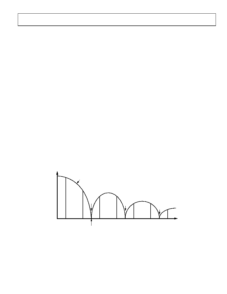
The AD9834 is a sampled signal with its output following
Nyquist sampling theorem. Specifically, its output spectrum
contains the fundamental plus aliased signals (images) that
occur at multiples of the reference clock frequency and the
selected output frequency. A graphical representation of the
sampled spectrum, with aliased images, is shown in Figure 28.
The prominence of the aliased images is dependent on the ratio
of fOUT to MCLK. If ratio is small, the aliased images are very
prominent and of a relatively high energy level as determined
by the sin(x)/x roll-off of the quantized DAC output. In fact,
depending on the fOUT/reference clock relationship, the first
aliased image can be on the order of 3 dB below the
fundamental.
A low-pass filter is generally placed between the output of the
DAC and the input of the comparator to further suppress the
effects of aliased images. Obviously, consideration must be
given to the relationship of the selected output frequency and
the reference clock frequency to avoid unwanted (and unexpected)
output anomalies. To apply the AD9834 as a clock generator,
limit the selected output frequency to <33% of reference clock
frequency, and thereby avoid generating aliased signals that fall
within, or close to, the output band of interest (generally dc-
selected output frequency). This practice eases the complexity
(and cost) of the external filter requirement for the clock
generator application. Refer to the AN-837 Application Note
for more information.
To enable the comparator, Bit SIGN/PIB and Bit OPBITEN in
the control resister are set to 1. This is explained further in
REGULATOR
The AD9834 has separate power supplies for the analog and
digital sections. AVDD provides the power supply required for
the analog section, and DVDD provides the power supply for
the digital section. Both of these supplies can have a value of
2.3 V to 5.5 V and are independent of each other. For example,
the analog section can be operated at 5 V, and the digital section
can be operated at 3 V, or vice versa.
The internal digital section of the AD9834 is operated at 2.5 V.
An on-board regulator steps down the voltage applied at DVDD
to 2.5 V. The digital interface (serial port) of the AD9834 also
operates from DVDD. These digital signals are level shifted
within the AD9834 to make them 2.5 V compatible.
When the applied voltage at the DVDD pin of the AD9834 is
equal to or less than 2.7 V, Pin CAP/2.5V and Pin DVDD should
be tied together, thus bypassing the on-board regulator.
OUTPUT VOLTAGE COMPLIANCE
of 4 mA. The maximum output voltage from the AD9834 is
VDD 1.5 V. This is to ensure that the output impedance of
the internal switch does not change, affecting the spectral
performance of the part. For a minimum supply of 2.3 V, the
maximum output voltage is 0.8 V. Specifications in Table 1 are
guaranteed with an RSET of 6.8 k and an RLOAD of 200 .
02705-
040
SYSTEM CLOCK
fOUT
fC – fOUT
fC + fOUT
2
fC – fOUT
2
fC + fOUT
3
fC – fOUT
3
fC + fOUT
fC
0Hz
FIRST
IMAGE
SECOND
IMAGE
THIRD
IMAGE
FOURTH
IMAGE
FIFTH
IMAGE
SIXTH
IMAGE
2
fC
3
fC
FREQUENCY (Hz)
S
IGN
A
L
A
M
P
LITU
D
E
sin x/x ENVELOPE
x = π (f/fC)
Figure 28. The DAC Output Spectrum
Rev. D | Page 17 of 32
相关PDF资料 |
PDF描述 |
|---|---|
| MCF51EM256CLK | IC MCU 32BIT 256KB FLASH 80LQFP |
| VE-B1F-IW-B1 | CONVERTER MOD DC/DC 72V 100W |
| MC9S08JM32CQH | IC MCU 8BIT 32K FLASH 64-QFP |
| AD9833BRM-REEL7 | IC WAVEFORM GEN PROG 10-MSOP |
| MC908QC16CDTE | IC MCU 8BIT 16K FLASH 16-TSSOP |
相关代理商/技术参数 |
参数描述 |
|---|---|
| AD9834BRUZ-REEL7 | 功能描述:IC DDS 10BIT 50MHZ LP 20TSSOP RoHS:是 类别:集成电路 (IC) >> 接口 - 直接数字合成 (DDS) 系列:- 产品变化通告:Product Discontinuance 27/Oct/2011 标准包装:2,500 系列:- 分辨率(位):10 b 主 fclk:25MHz 调节字宽(位):32 b 电源电压:2.97 V ~ 5.5 V 工作温度:-40°C ~ 85°C 安装类型:表面贴装 封装/外壳:16-TSSOP(0.173",4.40mm 宽) 供应商设备封装:16-TSSOP 包装:带卷 (TR) |
| AD9834CRUZ | 功能描述:IC DDS 10BIT 75MHZ LP 20-TSSOP RoHS:是 类别:集成电路 (IC) >> 接口 - 直接数字合成 (DDS) 系列:- 产品变化通告:Product Discontinuance 27/Oct/2011 标准包装:2,500 系列:- 分辨率(位):10 b 主 fclk:25MHz 调节字宽(位):32 b 电源电压:2.97 V ~ 5.5 V 工作温度:-40°C ~ 85°C 安装类型:表面贴装 封装/外壳:16-TSSOP(0.173",4.40mm 宽) 供应商设备封装:16-TSSOP 包装:带卷 (TR) |
| AD9834CRUZ-REEL7 | 功能描述:IC DDS 10BIT 75MHZ LP 20-TSSOP RoHS:是 类别:集成电路 (IC) >> 接口 - 直接数字合成 (DDS) 系列:- 产品变化通告:Product Discontinuance 27/Oct/2011 标准包装:2,500 系列:- 分辨率(位):10 b 主 fclk:25MHz 调节字宽(位):32 b 电源电压:2.97 V ~ 5.5 V 工作温度:-40°C ~ 85°C 安装类型:表面贴装 封装/外壳:16-TSSOP(0.173",4.40mm 宽) 供应商设备封装:16-TSSOP 包装:带卷 (TR) |
| AD9835 | 制造商:AD 制造商全称:Analog Devices 功能描述:50 MHz CMOS Complete DDS |
| AD9835BRU | 功能描述:IC DDS DAC 10BIT 50MHZ 16-TSSOP RoHS:否 类别:集成电路 (IC) >> 接口 - 直接数字合成 (DDS) 系列:- 产品变化通告:Product Discontinuance 27/Oct/2011 标准包装:2,500 系列:- 分辨率(位):10 b 主 fclk:25MHz 调节字宽(位):32 b 电源电压:2.97 V ~ 5.5 V 工作温度:-40°C ~ 85°C 安装类型:表面贴装 封装/外壳:16-TSSOP(0.173",4.40mm 宽) 供应商设备封装:16-TSSOP 包装:带卷 (TR) |
发布紧急采购,3分钟左右您将得到回复。