- 您现在的位置:买卖IC网 > PDF目录10978 > AD9838ACPZ-RL (Analog Devices Inc)IC DDS 16MHZ LOW PWR 20LFCSP PDF资料下载
参数资料
| 型号: | AD9838ACPZ-RL |
| 厂商: | Analog Devices Inc |
| 文件页数: | 11/32页 |
| 文件大小: | 0K |
| 描述: | IC DDS 16MHZ LOW PWR 20LFCSP |
| 产品培训模块: | Direct Digital Synthesis Tutorial Series (1 of 7): Introduction Direct Digital Synthesizer Tutorial Series (7 of 7): DDS in Action Direct Digital Synthesis Tutorial Series (3 of 7): Angle to Amplitude Converter Direct Digital Synthesis Tutorial Series (6 of 7): SINC Envelope Correction Direct Digital Synthesis Tutorial Series (4 of 7): Digital-to-Analog Converter Direct Digital Synthesis Tutorial Series (2 of 7): The Accumulator |
| 标准包装: | 5,000 |
| 分辨率(位): | 10 b |
| 主 fclk: | 5MHz |
| 电源电压: | 2.3 V ~ 5.5 V |
| 工作温度: | -40°C ~ 125°C |
| 安装类型: | 表面贴装 |
| 封装/外壳: | 20-WFQFN 裸露焊盘,CSP |
| 供应商设备封装: | 20-LFCSP-WQ(4x4) |
| 包装: | 带卷 (TR) |
第1页第2页第3页第4页第5页第6页第7页第8页第9页第10页当前第11页第12页第13页第14页第15页第16页第17页第18页第19页第20页第21页第22页第23页第24页第25页第26页第27页第28页第29页第30页第31页第32页
AD9838
Rev. A | Page 19 of 32
FREQUENCY AND PHASE REGISTERS
The AD9838 contains two frequency registers and two phase
registers, which are described in Table 8.
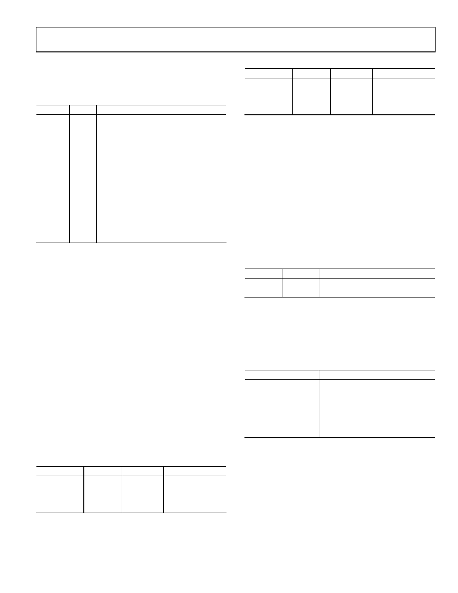
Table 8. Frequency and Phase Registers
Register
Size
Description
FREQ0
28 bits
Frequency Register 0.
When the FSEL bit or FSELECT pin = 0, the
FREQ0 register defines the output frequency
as a fraction of the MCLK frequency.
FREQ1
28 bits
Frequency Register 1.
When the FSEL bit or FSELECT pin = 1, the
FREQ1 register defines the output frequency
as a fraction of the MCLK frequency.
PHASE0
12 bits
Phase Offset Register 0.
When the PSEL bit or PSELECT pin = 0, the
contents of the PHASE0 register are added
to the output of the phase accumulator.
PHASE1
12 bits
Phase Offset Register 1.
When the PSEL bit or PSELECT pin = 1, the
contents of the PHASE1 register are added
to the output of the phase accumulator.
The analog output from the AD9838 is
fMCLK
/228 × FREQREG
where FREQREG is the value loaded into the selected frequency
register.
This signal is phase shifted by
2π/4096 × PHASEREG
where PHASEREG is the value contained in the selected phase
register.
The relationship of the selected output frequency and the refer-
ence clock frequency must be considered to avoid unwanted
output anomalies.
Selecting a Frequency or Phase Register
Access to the frequency and phase registers is controlled by
the FSELECT and PSELECT pins or by the FSEL and PSEL
control bits. If the PIN/SW control bit (Bit D9) = 1, the pins
control the function; if the PIN/SW control bit = 0, the bits
and PSEL bits are used, the pins should be held at CMOS logic
high or low. Control of the frequency and phase registers is
interchangeable from the pins to the bits.
Table 9. Selecting a Frequency Register
FSELECT Pin
FSEL Bit
PIN/SW Bit
Selected Register
0
X
1
FREQ0
1
X
1
FREQ1
X
0
FREQ0
X
1
0
FREQ1
Table 10. Selecting a Phase Register
PSELECT Pin
PSEL Bit
PIN/SW Bit
Selected Register
0
X
1
PHASE0
1
X
1
PHASE1
X
0
PHASE0
X
1
0
PHASE1
The FSELECT and PSELECT pins are sampled on the internal
falling edge of MCLK. It is recommended that the data on these
pins not change within the time window of the falling edge of
MCLK (see Figure 3 for timing). If the FSELECT or PSELECT
pin changes value when a falling edge occurs, there is an uncer-
tainty of one MCLK cycle as it pertains to when control is
transferred to the other frequency/phase register.
selecting and writing to the frequency and phase registers of the
AD9838.
Writing to a Frequency Register
When writing to a frequency register, Bit D15 and Bit D14 of
the control register give the address of the frequency register
(see Table 11).
Table 11. Frequency Register Bits
D15
D14
D13 to D0
0
1
14 FREQ0 register bits
1
0
14 FREQ1 register bits
To change the entire contents of a frequency register, two consec-
utive writes to the same address must be performed because the
frequency registers are 28 bits wide. The first write contains the
14 LSBs, and the second write contains the 14 MSBs. For this
mode of operation, the B28 control bit (Bit D13) must be set
to 1. An example of a 28-bit write is shown in Table 12.
Table 12. Writing 0xFFFC000 to the FREQ0 Register
SDATA Input
Result of Input Word
0010 0000 0000 0000
Control word write
(D15, D14 = 00), B28 (D13) = 1,
HLB (D12) = X
0100 0000 0000 0000
FREQ0 register write
(D15, D14 = 01), 14 LSBs = 0x0000
0111 1111 1111 1111
FREQ0 register write
(D15, D14 = 01), 14 MSBs = 0x3FFF
Note, however, that continuous writes to the same frequency
register may result in intermediate updates during the writes. If
a frequency sweep, or something similar, is required, it is recom-
mended that users alternate between the two frequency registers.
相关PDF资料 |
PDF描述 |
|---|---|
| AD9837BCPZ-RL | IC WAVEFORM GEN PROG 10LFCSP |
| VE-2WM-IY-F2 | CONVERTER MOD DC/DC 10V 50W |
| AD9837ACPZ-RL | IC WAVEFORM GEN PROG 10LFCSP |
| VE-2W3-IY-F4 | CONVERTER MOD DC/DC 24V 50W |
| VE-2W2-IY-F3 | CONVERTER MOD DC/DC 15V 50W |
相关代理商/技术参数 |
参数描述 |
|---|---|
| AD9838ACPZ-RL7 | 功能描述:IC DDS 16MHZ LOW PWR 20LFCSP RoHS:是 类别:集成电路 (IC) >> 接口 - 直接数字合成 (DDS) 系列:- 产品变化通告:Product Discontinuance 27/Oct/2011 标准包装:2,500 系列:- 分辨率(位):10 b 主 fclk:25MHz 调节字宽(位):32 b 电源电压:2.97 V ~ 5.5 V 工作温度:-40°C ~ 85°C 安装类型:表面贴装 封装/外壳:16-TSSOP(0.173",4.40mm 宽) 供应商设备封装:16-TSSOP 包装:带卷 (TR) |
| AD9838BCPZ-RL | 功能描述:IC DDS 16MHZ LOW PWR 20LFCSP RoHS:是 类别:集成电路 (IC) >> 接口 - 直接数字合成 (DDS) 系列:- 产品变化通告:Product Discontinuance 27/Oct/2011 标准包装:2,500 系列:- 分辨率(位):10 b 主 fclk:25MHz 调节字宽(位):32 b 电源电压:2.97 V ~ 5.5 V 工作温度:-40°C ~ 85°C 安装类型:表面贴装 封装/外壳:16-TSSOP(0.173",4.40mm 宽) 供应商设备封装:16-TSSOP 包装:带卷 (TR) |
| AD9838BCPZ-RL7 | 功能描述:IC DDS 16MHZ LP 20LFCSP RoHS:是 类别:集成电路 (IC) >> 接口 - 直接数字合成 (DDS) 系列:- 产品变化通告:Product Discontinuance 27/Oct/2011 标准包装:2,500 系列:- 分辨率(位):10 b 主 fclk:25MHz 调节字宽(位):32 b 电源电压:2.97 V ~ 5.5 V 工作温度:-40°C ~ 85°C 安装类型:表面贴装 封装/外壳:16-TSSOP(0.173",4.40mm 宽) 供应商设备封装:16-TSSOP 包装:带卷 (TR) |
| AD9840 | 制造商:AD 制造商全称:Analog Devices 功能描述:Complete 10-Bit 40 MSPS CCD Signal Processor |
| AD9840A | 制造商:AD 制造商全称:Analog Devices 功能描述:Complete 10-Bit 40 MSPS CCD Signal Processor |
发布紧急采购,3分钟左右您将得到回复。