- 您现在的位置:买卖IC网 > PDF目录11674 > AD9845BJSTZ (Analog Devices Inc)IC CCD SIGNAL PROC 12BIT 48-LQFP PDF资料下载
参数资料
| 型号: | AD9845BJSTZ |
| 厂商: | Analog Devices Inc |
| 文件页数: | 11/24页 |
| 文件大小: | 0K |
| 描述: | IC CCD SIGNAL PROC 12BIT 48-LQFP |
| 标准包装: | 1 |
| 类型: | CCD 信号处理器,12 位 |
| 输入类型: | 逻辑 |
| 输出类型: | 逻辑 |
| 接口: | 3 线串口 |
| 安装类型: | 表面贴装 |
| 封装/外壳: | 48-LQFP |
| 供应商设备封装: | 48-LQFP(7x7) |
| 包装: | 托盘 |
| 产品目录页面: | 776 (CN2011-ZH PDF) |
REV.
B
AD9845B
–19–
AUX1IN
0.1 F
VGA GAIN
REGISTER
ADC
VGA
10
5k
0.4V
INPUT SIGNAL
??V
0.8V
0.4V
MIDSCALE
0dB TO 36dB
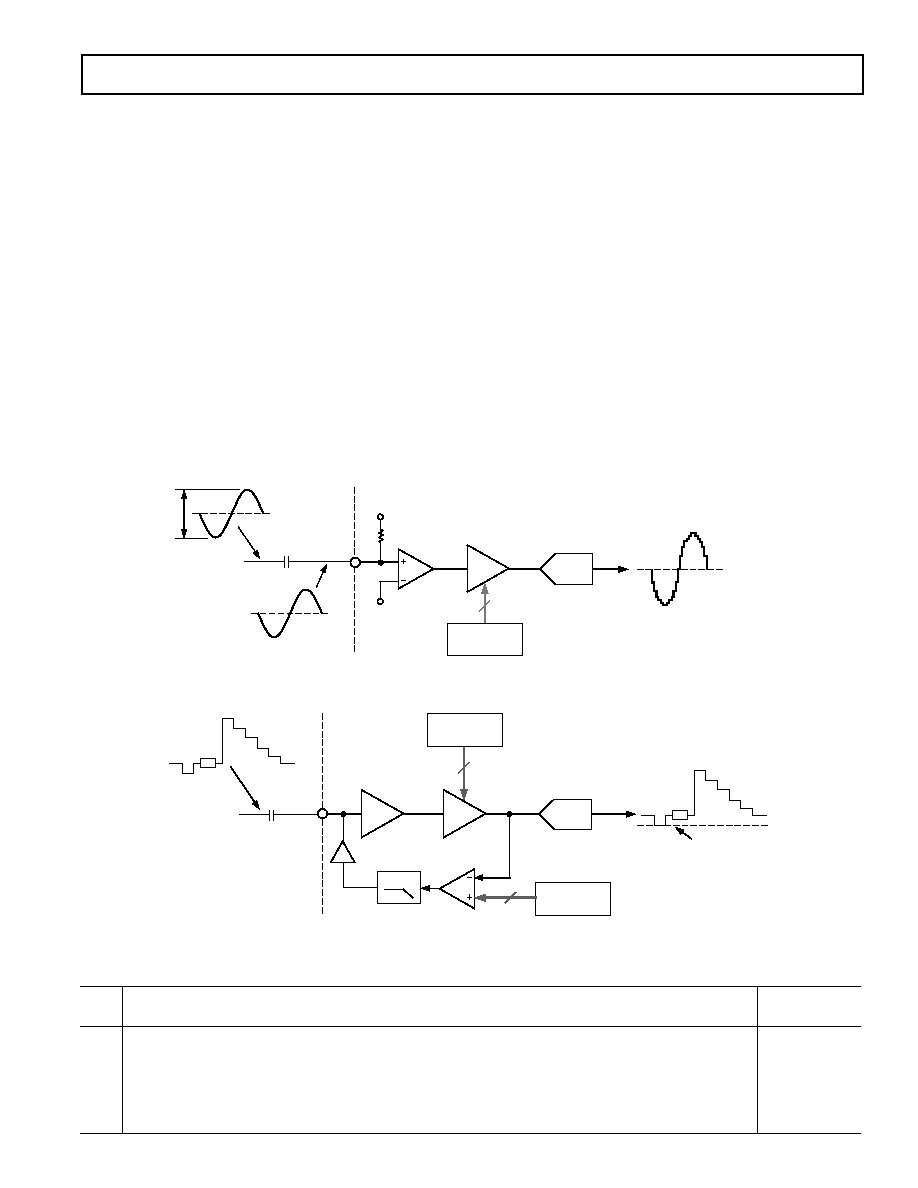
Figure 30. AUX1 Circuit Configuration
0dB TO 18dB
8
AUX2IN
BUFFER
0.1 F
VIDEO
SIGNAL
9
CLAMP LEVEL
LPF
VGA GAIN
REGISTER
ADC
VGA
VIDEO CLAMP
CIRCUIT
CLAMP LEVEL
REGISTER
Figure 31. AUX2 Circuit Configuration
Table VII. VGA Gain Register Used for AUX2 Mode
MSB
LSB
D10
D9
D8
D7
D6
D5
D4
D3
D2
D1
D0
Gain (dB)
X0
XXXXXXXXX0.0
10000000000.0
∑∑
111111111118.0
be used, but clamp noise may increase and the ability to track
low frequency variations in the black level will be reduced.
A/D Converter
The AD9845B uses high performance ADC architecture, opti-
mized for high speed and low power. Differential nonlinearity
(DNL) performance is typically better than 0.5 LSB, as shown in
TPC 2. Instead of the 1 V full-scale range used by the earlier
AD9801 and AD9803 products from Analog Devices, the
AD9845B’s ADC uses a 2 V input range. Better noise perfor-
mance results from using a larger ADC full-scale range
(see TPC 3).
AUX1 Mode
For applications that do not require CDS, the AD9845B can be
configured to sample ac-coupled waveforms. Figure 30 shows
the circuit configuration for using the AUX1 channel input
(Pin 36). A single 0.1
mF ac-coupling capacitor is needed between
the input signal driver and the AUX1IN pin. An on-chip dc bias
circuit sets the average value of the input signal to approximately
0.4 V, which is referenced to the midscale code of the ADC.
The VGA gain register provides a gain range of 0 dB to 36 dB in
this mode of operation (see Figure 29). The VGA gains up the
signal level with respect to the 0.4 V bias level. Signal levels
above the bias level will be further increased to a higher ADC
code, while signal levels below the bias level will be further
decreased to a lower ADC code.
AUX2 Mode
For sampling video-type waveforms, such as NTSC and PAL
signals, the AUX2 channel provides black level clamping, gain
adjustment, and A/D conversion. Figure 31 shows the circuit
configuration for using the AUX2 channel input (Pin 34). An
external 0.1
mF blocking capacitor is used with the on-chip video
clamp circuit to level shift the input signal to a desired refer-
ence level. The clamp circuit automatically senses the most
negative portion of the input signal and adjusts the voltage
across the input capacitor. This forces the black level of the
input signal to be equal to the value programmed into the clamp
level register (see the Serial Interface Timing and Internal Register
Description section). The VGA provides gain adjustment from
0 dB to 18 dB. The same VGA gain register is used, but only
the 9 MSBs of the gain register are used (see Table VII.)
相关PDF资料 |
PDF描述 |
|---|---|
| 3-1478978-1 | CONN JACK SMA 50 OHM R/A PCB |
| AD9949AKCPZ | IC CCD SIGNAL PROCESSOR 40-LFCSP |
| VE-J3K-IY-F2 | CONVERTER MOD DC/DC 40V 50W |
| AD694JNZ | IC TRANSMITTER 4-20MA 16-DIP |
| VE-J3K-IY-F1 | CONVERTER MOD DC/DC 40V 50W |
相关代理商/技术参数 |
参数描述 |
|---|---|
| AD9845BJSTZKL1 | 制造商:Analog Devices 功能描述: |
| AD9845BJSTZRL | 功能描述:IC CCD SIGNAL PROC 12BIT 48LQFP RoHS:是 类别:集成电路 (IC) >> 接口 - 传感器和探测器接口 系列:- 其它有关文件:Automotive Product Guide 产品培训模块:Lead (SnPb) Finish for COTS Obsolescence Mitigation Program 标准包装:74 系列:- 类型:触控式传感器 输入类型:数字 输出类型:数字 接口:JTAG,串行 电流 - 电源:100µA 安装类型:表面贴装 封装/外壳:20-TSSOP(0.173",4.40mm 宽) 供应商设备封装:20-TSSOP 包装:管件 |
| AD9846A | 制造商:AD 制造商全称:Analog Devices 功能描述:Complete 10-Bit 30 MSPS CCD Signal Processor |
| AD9846AJST | 制造商:Analog Devices 功能描述:AFE VID 1ADC 10-BIT 3.3V 48LQFP - Bulk 制造商:Rochester Electronics LLC 功能描述:10 BIT 30 MSPS CCD SIGNAL PROCESSOR - Tape and Reel |
| AD9846AJSTRL | 制造商:Analog Devices 功能描述:AFE VID 1ADC 10-BIT 3.3V 48LQFP - Tape and Reel 制造商:Rochester Electronics LLC 功能描述:10 BIT 30 MSPS CCD SIGNAL PROCESSOR - Tape and Reel |
发布紧急采购,3分钟左右您将得到回复。