- 您现在的位置:买卖IC网 > PDF目录10977 > AD9850BRSZ-REEL (Analog Devices Inc)IC DDS SYNTHESIZER CMOS 28-SSOP PDF资料下载
参数资料
| 型号: | AD9850BRSZ-REEL |
| 厂商: | Analog Devices Inc |
| 文件页数: | 5/20页 |
| 文件大小: | 0K |
| 描述: | IC DDS SYNTHESIZER CMOS 28-SSOP |
| 产品培训模块: | Direct Digital Synthesis Tutorial Series (1 of 7): Introduction Direct Digital Synthesizer Tutorial Series (7 of 7): DDS in Action Direct Digital Synthesis Tutorial Series (3 of 7): Angle to Amplitude Converter Direct Digital Synthesis Tutorial Series (6 of 7): SINC Envelope Correction Direct Digital Synthesis Tutorial Series (4 of 7): Digital-to-Analog Converter Direct Digital Synthesis Tutorial Series (2 of 7): The Accumulator |
| 标准包装: | 1,500 |
| 分辨率(位): | 10 b |
| 主 fclk: | 125MHz |
| 调节字宽(位): | 32 b |
| 电源电压: | 3.3V,5V |
| 工作温度: | -40°C ~ 85°C |
| 安装类型: | 表面贴装 |
| 封装/外壳: | 28-SSOP(0.209",5.30mm 宽) |
| 供应商设备封装: | 28-SSOP |
| 包装: | 带卷 (TR) |
AD9850
–13–
REV. H
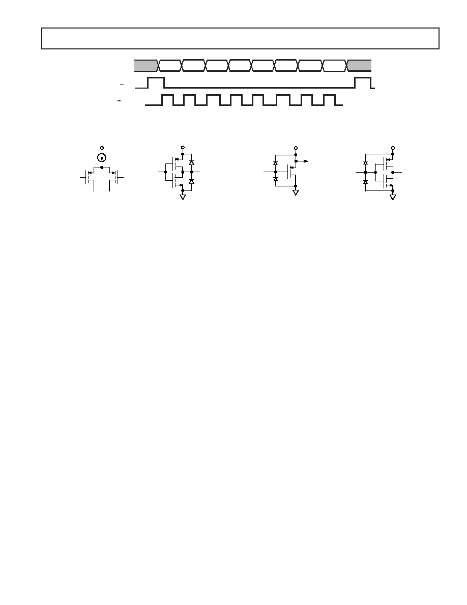
DATA (7) –
W CLK
FQ UD
W32 = 0
W33 = 0
W34 = 1
W35 = X
W36 = X
W37 = X
W38 = X
W39 = X
Figure 13. Serial Load Power-Down Sequence
VCC
QOUT/
QOUTB
VCC
IOUT IOUTB
VINP/
VINN
VCC
DIGITAL
IN
VCC
DAC Output
Comparator Output
Comparator Input
Digital Inputs
Figure 14. AD9850 I/O Equivalent Circuits
PCB LAYOUT INFORMATION
The AD9850/CGPCB and AD9850/FSPCB evaluation boards
(Figures 15 through 18) represent typical implementations of the
AD9850 and exemplify the use of high frequency/high resolution
design and layout practices. The printed circuit board that contains
the AD9850 should be a multilayer board that allows dedicated
power and ground planes. The power and ground planes should
be free of etched traces that cause discontinuities in the planes. It
is recommended that the top layer of the multilayer board also
contain an interspatial ground plane, which makes ground avail-
able for surface-mount devices. If separate analog and digital
system ground planes exist, they should be connected together at
the AD9850 for optimum results.
Avoid running digital lines under the device because these
couple noise onto the die. The power supply lines to the
AD9850 should use as large a track as possible to provide a low
impedance path and reduce the effects of glitches on the power
supply line. Fast switching signals like clocks should be shielded
with ground to avoid radiating noise to other sections of the
board. Avoid crossover of digital and analog signal paths. Traces
on opposite sides of the board should run at right angles to each
other. This reduces the effects of feedthrough through the cir-
cuit board. Use microstrip techniques where possible.
Good decoupling is also an important consideration. The analog
(AVDD) and digital (DVDD) supplies to the AD9850 are
independent and separately pinned out to minimize coupling
between analog and digital sections of the device. All analog
and digital supplies should be decoupled to AGND and DGND,
respectively, with high quality ceramic capacitors. To achieve
best performance from the decoupling capacitors, they should
be placed as close as possible to the device, ideally right up
against the device. In systems where a common supply is used to
drive both the AVDD and DVDD supplies of the AD9850, it is
recommended that the system’s AVDD supply be used.
Analog Devices, Inc. applications engineering support is avail-
able to answer additional questions on grounding and PCB
layout. Call 1-800-ANALOGD or contact us at
www.analog.com/dds.
Evaluation Boards
Two versions of evaluation boards are available for the AD9850,
which facilitate the implementation of the device for bench-
top analysis and serve as a reference for PCB layout. The
AD9850/FSPCB is used in applications where the device is used
primarily as a frequency synthesizer. This version facilitates
connection of the AD9850’s internal D/A converter output to a
50
spectrum analyzer input; the internal comparator on the
AD9850 DUT is not enabled (see Figure 15 for an electrical
schematic of AD9850/FSPCB). The AD9850/CGPCB is used
in applications using the device in the clock generator mode. It
connects the AD9850’s DAC output to the internal comparator
input via a single-ended, 42 MHz low-pass, 5-pole elliptical
filter. This model facilitates the access of the AD9850’s com-
parator output for evaluation of the device as a frequency- and
phase-agile clock source (see Figure 17 for an electrical sche-
matic of AD9850/CGPCB).
Both versions of the AD9850 evaluation board are designed to
interface to the parallel printer port of a PC. The operating
software runs under Microsoft
Windows and provides a user-
friendly and intuitive format for controlling the functionality
and observing the performance of the device. The 3.5 inch
floppy provided with the evaluation board contains an execut-
able file that loads and displays the AD9850 function-selection
screen. The evaluation board can be operated with 3.3 V or 5 V
supplies. The evaluation boards are configured at the factory for
an external reference clock input; if the on-board crystal clock
source is used, remove R2.
相关PDF资料 |
PDF描述 |
|---|---|
| VE-BW1-IY-F2 | CONVERTER MOD DC/DC 12V 50W |
| VE-BW0-IY-F2 | CONVERTER MOD DC/DC 5V 50W |
| VE-B1X-IY-F3 | CONVERTER MOD DC/DC 5.2V 50W |
| VE-B1W-IY-F3 | CONVERTER MOD DC/DC 5.5V 50W |
| VE-B1R-IY-F3 | CONVERTER MOD DC/DC 7.5V 50W |
相关代理商/技术参数 |
参数描述 |
|---|---|
| AD9851 | 制造商:AD 制造商全称:Analog Devices 功能描述:CMOS 180 MHz DDS/DAC Synthesizer |
| AD9851/CGPCB | 制造商:Analog Devices 功能描述:NCO/DDS, CMOS 180MHZ DDS/DAC SYNTHESIZER - Bulk 制造商:Rochester Electronics LLC 功能描述:DDS CLOCK DRIVER - Bulk |
| AD9851/FSPCB | 制造商:Analog Devices 功能描述:Evaluation Board For NCO/DDS, CMOS 180MHZ DDS/DAC Synthesizer 制造商:Analog Devices 功能描述:NCO/DDS, CMOS 180MHZ DDS/DAC SYNTHESIZER - Bulk |
| AD9851BRS | 功能描述:IC DDS DAC W/COMP 180MHZ 28-SSOP RoHS:否 类别:集成电路 (IC) >> 接口 - 直接数字合成 (DDS) 系列:- 产品变化通告:Product Discontinuance 27/Oct/2011 标准包装:2,500 系列:- 分辨率(位):10 b 主 fclk:25MHz 调节字宽(位):32 b 电源电压:2.97 V ~ 5.5 V 工作温度:-40°C ~ 85°C 安装类型:表面贴装 封装/外壳:16-TSSOP(0.173",4.40mm 宽) 供应商设备封装:16-TSSOP 包装:带卷 (TR) |
| AD9851BRSRL | 功能描述:IC DDS/DAC SYNTHESIZER 28-SSOP RoHS:否 类别:集成电路 (IC) >> 接口 - 直接数字合成 (DDS) 系列:- 产品变化通告:Product Discontinuance 27/Oct/2011 标准包装:2,500 系列:- 分辨率(位):10 b 主 fclk:25MHz 调节字宽(位):32 b 电源电压:2.97 V ~ 5.5 V 工作温度:-40°C ~ 85°C 安装类型:表面贴装 封装/外壳:16-TSSOP(0.173",4.40mm 宽) 供应商设备封装:16-TSSOP 包装:带卷 (TR) |
发布紧急采购,3分钟左右您将得到回复。