参数资料
| 型号: | AD9851BRS |
| 厂商: | Analog Devices Inc |
| 文件页数: | 1/24页 |
| 文件大小: | 0K |
| 描述: | IC DDS DAC W/COMP 180MHZ 28-SSOP |
| 产品培训模块: | Direct Digital Synthesis Tutorial Series (1 of 7): Introduction Direct Digital Synthesizer Tutorial Series (7 of 7): DDS in Action Direct Digital Synthesis Tutorial Series (3 of 7): Angle to Amplitude Converter Direct Digital Synthesis Tutorial Series (6 of 7): SINC Envelope Correction Direct Digital Synthesis Tutorial Series (4 of 7): Digital-to-Analog Converter Direct Digital Synthesis Tutorial Series (2 of 7): The Accumulator |
| 标准包装: | 1 |
| 分辨率(位): | 10 b |
| 主 fclk: | 180MHz |
| 调节字宽(位): | 32 b |
| 电源电压: | 2.7 V ~ 5.25 V |
| 工作温度: | -40°C ~ 85°C |
| 安装类型: | 表面贴装 |
| 封装/外壳: | 28-SSOP(0.209",5.30mm 宽) |
| 供应商设备封装: | 28-SSOP |
| 包装: | 管件 |
Information furnished by Analog Devices is believed to be accurate and
reliable. However, no responsibility is assumed by Analog Devices for its
use, nor for any infringements of patents or other rights of third parties
that may result from its use. No license is granted by implication or oth-
erwise under any patent or patent rights of Analog Devices.Trademarks
and registered trademarks are the property of their respective owners.
One Technology Way, P.O. Box 9106, Norwood, MA 02062-9106, U.S.A.
Tel: 781/329-4700
Fax: 781/326-8703
2004 Analog Devices, Inc. All rights reserved.
AD9851
CMOS 180 MHz
DDS/DAC Synthesizer
FEATURES
180 MHz Clock Rate with Selectable 6 Reference Clock
Multiplier
On-Chip High Performance 10-Bit DAC and High Speed
Comparator with Hysteresis
SFDR >43 dB @ 70 MHz AOUT
32-Bit Frequency Tuning Word
Simplified Control Interface: Parallel or Serial
Asynchronous Loading Format
5-Bit Phase Modulation and Offset Capability
Comparator Jitter <80 ps p-p @ 20 MHz
2.7 V to 5.25 V Single-Supply Operation
Low Power: 555 mW @ 180 MHz
Power-Down Function, 4 mW @ 2.7 V
Ultrasmall 28-Lead SSOP Packaging
APPLICATIONS
Frequency/Phase-Agile Sine Wave Synthesis
Clock Recovery and Locking Circuitry for Digital
Communications
Digitally Controlled ADC Encode Generator
Agile Local Oscillator Applications in Communications
Quadrature Oscillator
CW, AM, FM, FSK, MSK Mode Transmitter
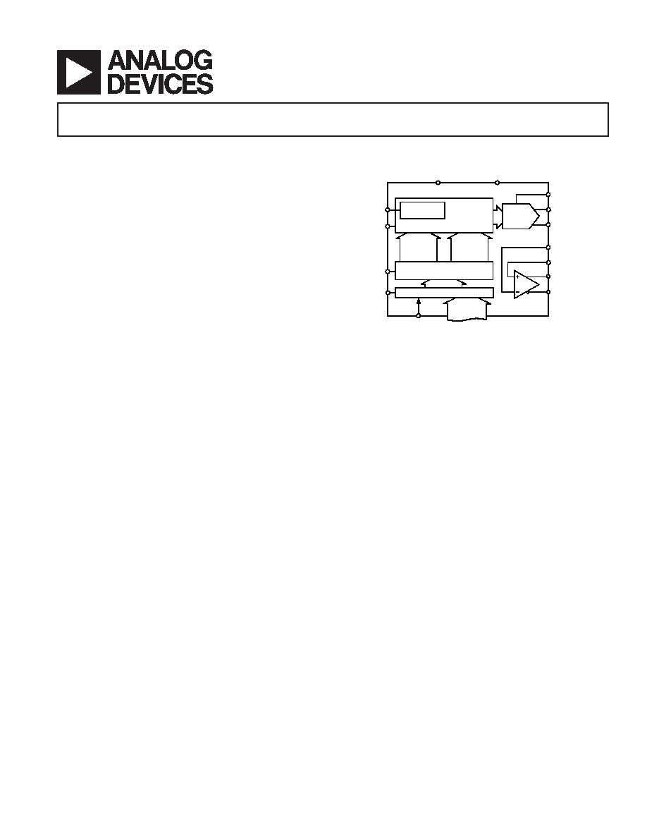
FUNCTIONAL BLOCK DIAGRAM
32-BIT
TUNING
WORD
PHASE
AND
CONTROL
WORDS
FREQUENCY/PHASE
DATA REGISTER
DATA INPUT REGISTER
10-BIT
DAC
DAC RSET
ANALOG
OUT
ANALOG
IN
CLOCK OUT
HIGH SPEED
DDS
FREQUENCY
UPDATE/DATA
REGISTER
RESET
WORD LOAD
CLOCK
MASTER
RESET
REF
CLOCK IN
6 REFCLK
MULTIPLIER
COMPARATOR
SERIAL
LOAD
1 BIT
40 LOADS
PARALLEL
LOAD
8 BITS
5 LOADS
FREQUENCY, PHASE
AND CONTROL DATA INPUT
AD9851
+VS
GND
GENERAL DESCRIPTION
The AD9851 is a highly integrated device that uses advanced
DDS technology, coupled with an internal high speed, high
performance D/A converter, and comparator, to form a digitally
programmable frequency synthesizer and clock generator func-
tion. When referenced to an accurate clock source, the AD9851
generates a stable frequency and phase-programmable digitized
analog output sine wave. This sine wave can be used directly as
a frequency source, or internally converted to a square wave for
agile-clock generator applications. The AD9851’s innovative
high speed DDS core accepts a 32-bit frequency tuning word,
which results in an output tuning resolution of approximately
0.04 Hz with a 180 MHz system clock. The AD9851 contains
a unique 6 REFCLK Multiplier circuit that eliminates the
need for a high speed reference oscillator. The 6 REFCLK
Multiplier has minimal impact on SFDR and phase noise char-
acteristics. The AD9851 provides five bits of programmable
phase modulation resolution to enable phase shifting of its
output in increments of 11.25°.
The AD9851 contains an internal high speed comparator that
can be configured to accept the (externally) filtered output of the
DAC to generate a low jitter output pulse.
The frequency tuning, control, and phase modulation words are
asynchronously loaded into the AD9851 via a parallel or serial
loading format. The parallel load format consists of five iterative
loads of an 8-bit control word (byte). The first 8-bit byte controls
output phase, 6 REFCLK Multiplier, power-down enable and
loading format; the remaining bytes comprise the 32-bit frequency
tuning word. Serial loading is accomplished via a 40-bit serial data
stream entering through one of the parallel input bus lines. The
AD9851 uses advanced CMOS technology to provide this break-
through level of functionality on just 555 mW of power dissipation
(5 V supply), at the maximum clock rate of 180 MHz.
The AD9851 is available in a space-saving 28-lead SSOP,
surface-mount package that is pin-for-pin compatible with the
popular AD9850 125 MHz DDS. It is specified to operate over
the extended industrial temperature range of –40°C to +85°C
at >3.0 V supply voltage. Below 3.0 V, the specifications apply
over the commercial temperature range of 0°C to 85°C.
REV. D
相关PDF资料 |
PDF描述 |
|---|---|
| AD9852ASVZ | IC DDS SYNTHESIZER CMOS 80-TQFP |
| AD9854ASTZ | IC DDS QUADRATURE CMOS 80-LQFP |
| AD9858BSVZ | IC DDS DAC 10BIT 1GSPS 100-TQFP |
| AD9859YSVZ-REEL7 | IC DDS DAC 10BIT 400MSPS 48TQFP |
| AD9880KSTZ-100 | IC INTERFACE/HDMI 100MHZ 100LQFP |
相关代理商/技术参数 |
参数描述 |
|---|---|
| AD9851BRSRL | 功能描述:IC DDS/DAC SYNTHESIZER 28-SSOP RoHS:否 类别:集成电路 (IC) >> 接口 - 直接数字合成 (DDS) 系列:- 产品变化通告:Product Discontinuance 27/Oct/2011 标准包装:2,500 系列:- 分辨率(位):10 b 主 fclk:25MHz 调节字宽(位):32 b 电源电压:2.97 V ~ 5.5 V 工作温度:-40°C ~ 85°C 安装类型:表面贴装 封装/外壳:16-TSSOP(0.173",4.40mm 宽) 供应商设备封装:16-TSSOP 包装:带卷 (TR) |
| AD9851BRSZ | 功能描述:IC SYNTHESIZER DDS/DAC 28-SSOP RoHS:是 类别:集成电路 (IC) >> 接口 - 直接数字合成 (DDS) 系列:- 产品变化通告:Product Discontinuance 27/Oct/2011 标准包装:2,500 系列:- 分辨率(位):10 b 主 fclk:25MHz 调节字宽(位):32 b 电源电压:2.97 V ~ 5.5 V 工作温度:-40°C ~ 85°C 安装类型:表面贴装 封装/外壳:16-TSSOP(0.173",4.40mm 宽) 供应商设备封装:16-TSSOP 包装:带卷 (TR) |
| AD9851BRSZ | 制造商:Analog Devices 功能描述:Direct Digital Synthesizer IC (DDS) |
| AD9851BRSZRL | 功能描述:IC SYNTHESR DDS/DAC 28SSOP TR RoHS:是 类别:集成电路 (IC) >> 接口 - 直接数字合成 (DDS) 系列:- 产品变化通告:Product Discontinuance 27/Oct/2011 标准包装:2,500 系列:- 分辨率(位):10 b 主 fclk:25MHz 调节字宽(位):32 b 电源电压:2.97 V ~ 5.5 V 工作温度:-40°C ~ 85°C 安装类型:表面贴装 封装/外壳:16-TSSOP(0.173",4.40mm 宽) 供应商设备封装:16-TSSOP 包装:带卷 (TR) |
| AD9851CGPCB | 制造商:AD 制造商全称:Analog Devices 功能描述:CMOS 180 MHz DDS/DAC Synthesizer |
发布紧急采购,3分钟左右您将得到回复。