参数资料
| 型号: | AD9851BRS |
| 厂商: | Analog Devices Inc |
| 文件页数: | 18/24页 |
| 文件大小: | 0K |
| 描述: | IC DDS DAC W/COMP 180MHZ 28-SSOP |
| 产品培训模块: | Direct Digital Synthesis Tutorial Series (1 of 7): Introduction Direct Digital Synthesizer Tutorial Series (7 of 7): DDS in Action Direct Digital Synthesis Tutorial Series (3 of 7): Angle to Amplitude Converter Direct Digital Synthesis Tutorial Series (6 of 7): SINC Envelope Correction Direct Digital Synthesis Tutorial Series (4 of 7): Digital-to-Analog Converter Direct Digital Synthesis Tutorial Series (2 of 7): The Accumulator |
| 标准包装: | 1 |
| 分辨率(位): | 10 b |
| 主 fclk: | 180MHz |
| 调节字宽(位): | 32 b |
| 电源电压: | 2.7 V ~ 5.25 V |
| 工作温度: | -40°C ~ 85°C |
| 安装类型: | 表面贴装 |
| 封装/外壳: | 28-SSOP(0.209",5.30mm 宽) |
| 供应商设备封装: | 28-SSOP |
| 包装: | 管件 |
AD9851
–3–
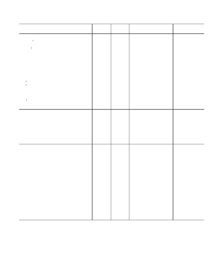
Test
AD9851BRS
Parameter
Temp
Level
Min
Typ
Max
Unit
TIMING CHARACTERISTICS4
tWH, tWL (W_CLK Min Pulse Width High/Low)
WL
Full
IV
3.5
ns
tDS, tDH (Data to W_CLK Setup and Hold Times)
Full
IV
3.5
ns
tFH, tFL (FQ_UD Min Pulse Width High/Low)
FL
Full
IV
7
ns
tCD (REFCLK Delay After FQ_UD)5
Full
IV
3.5
ns
tFD (FQ_UD Min Delay After W_CLK)
Full
IV
7
ns
tCF (Output Latency from FQ_UD)
Frequency Change
Full
IV
18
SYSCLK
Cycles
Phase Change
Full
IV
13
SYSCLK
Cycles
tRH (CLKIN Delay After RESET Rising Edge)
Full
IV
3.5
ns
tRL (RESET Falling Edge After CLKIN)
RL
Full
IV
3.5
ns
tRR (Recovery from RESET)
RR
Full
IV
2
SYSCLK
Cycles
tRS (Minimum RESET Width)
Full
IV
5
SYSCLK
Cycles
tOL (RESET Output Latency)
OL
Full
IV
13
SYSCLK
Cycles
Wake-Up Time from Power-Down Mode6
25°C
V
5
s
CMOS LOGIC INPUTS
Logic 1 Voltage, 5 V Supply
25°C
I
3.5
V
Logic 1 Voltage, 3.3 V Supply
25°C
IV
2.4
V
Logic 1 Voltage, 2.7 V Supply
25°C
IV
2.0
V
Logic 0 Voltage
25°C
IV
0.8
V
Logic 1 Current
25°C
I
12
A
Logic 0 Current
25°C
I
12
A
Rise/Fall Time
25°C
IV
100
ns
Input Capacitance
25°C
V
3
pF
POWER SUPPLY
VS6 Current @:
62.5 MHz Clock, 2.7 V Supply
25°C
VI
30
35
mA
100 MHz Clock, 2.7 V Supply
25°C
VI
40
50
mA
62.5 MHz Clock, 3.3 V Supply
25°C
VI
35
45
mA
125 MHz Clock, 3.3 V Supply
25°C
VI
55
70
mA
62.5 MHz Clock, 5 V Supply
25°C
VI
50
65
mA
125 MHz Clock, 5 V Supply
25°C
VI
70
90
mA
180 MHz Clock, 5 V Supply
25°C
VI
110
130
mA
Power Dissipation @ :
62.5 MHz Clock, 5 V Supply
25°C
VI
250
325
mW
62.5 MHz Clock, 3.3 V Supply
25°C
VI
115
150
mW
62.5 MHz Clock, 2.7 V Supply
25°C
VI
85
95
mW
100 MHz Clock, 2.7 V Supply
25°C
VI
110
135
mW
125 MHz Clock, 5 V Supply
25°C
VI
365
450
mW
125 MHz Clock, 3.3 V Supply
25°C
VI
180
230
mW
180 MHz Clock, 5 V Supply
25°C
VI
555
650
mW
PDISS Power-Down Mode @:
5 V Supply
25°C
VI
17
55
mW
2.7 V Supply
25°C
VI
4
20
mW
NOTES
1+VS collectively refers to the positive voltages applied to DVDD, PVCC, and AVDD.Voltages applied to these pins should be of the same potential.
2Indicates the minimum signal levels required to reliably clock the device at the indicated supply voltages.This specifies the p-p signal level and dc offset needed when the
clocking signal is not of CMOS/TTL origin, i.e., a sine wave with 0 V dc offset.
3The comparator’s jitter contribution to any input signal.This is the minimum jitter on the outputs that can be expected from an ideal input. Considerably more output
jitter is seen when nonideal input signals are presented to the comparator inputs. Nonideal characteristics include the presence of extraneous, nonharmonic signals (spur’s,
noise), slower slew rate, and low comparator overdrive.
4Timing of input signals FQ_UD,WCLK, RESET are asynchronous to the reference clock; however, the presence of a reference clock is required to implement those
functions. In the absence of a reference clock, the AD9851 automatically enters power-down mode rendering the IC, including the comparator, inoperable until a refer-
ence clock is restored.Very high speed updates of frequency/phase word will require FQ_UD and WCLK to be externally synchronized with the external reference clock to
ensure proper timing.
5Not applicable when 6 REFCLK Multiplier is engaged.
6Assumes no capacitive load on DACBP (Pin 17).
Specifications subject to change without notice.
REV. D
相关PDF资料 |
PDF描述 |
|---|---|
| AD9852ASVZ | IC DDS SYNTHESIZER CMOS 80-TQFP |
| AD9854ASTZ | IC DDS QUADRATURE CMOS 80-LQFP |
| AD9858BSVZ | IC DDS DAC 10BIT 1GSPS 100-TQFP |
| AD9859YSVZ-REEL7 | IC DDS DAC 10BIT 400MSPS 48TQFP |
| AD9880KSTZ-100 | IC INTERFACE/HDMI 100MHZ 100LQFP |
相关代理商/技术参数 |
参数描述 |
|---|---|
| AD9851BRSRL | 功能描述:IC DDS/DAC SYNTHESIZER 28-SSOP RoHS:否 类别:集成电路 (IC) >> 接口 - 直接数字合成 (DDS) 系列:- 产品变化通告:Product Discontinuance 27/Oct/2011 标准包装:2,500 系列:- 分辨率(位):10 b 主 fclk:25MHz 调节字宽(位):32 b 电源电压:2.97 V ~ 5.5 V 工作温度:-40°C ~ 85°C 安装类型:表面贴装 封装/外壳:16-TSSOP(0.173",4.40mm 宽) 供应商设备封装:16-TSSOP 包装:带卷 (TR) |
| AD9851BRSZ | 功能描述:IC SYNTHESIZER DDS/DAC 28-SSOP RoHS:是 类别:集成电路 (IC) >> 接口 - 直接数字合成 (DDS) 系列:- 产品变化通告:Product Discontinuance 27/Oct/2011 标准包装:2,500 系列:- 分辨率(位):10 b 主 fclk:25MHz 调节字宽(位):32 b 电源电压:2.97 V ~ 5.5 V 工作温度:-40°C ~ 85°C 安装类型:表面贴装 封装/外壳:16-TSSOP(0.173",4.40mm 宽) 供应商设备封装:16-TSSOP 包装:带卷 (TR) |
| AD9851BRSZ | 制造商:Analog Devices 功能描述:Direct Digital Synthesizer IC (DDS) |
| AD9851BRSZRL | 功能描述:IC SYNTHESR DDS/DAC 28SSOP TR RoHS:是 类别:集成电路 (IC) >> 接口 - 直接数字合成 (DDS) 系列:- 产品变化通告:Product Discontinuance 27/Oct/2011 标准包装:2,500 系列:- 分辨率(位):10 b 主 fclk:25MHz 调节字宽(位):32 b 电源电压:2.97 V ~ 5.5 V 工作温度:-40°C ~ 85°C 安装类型:表面贴装 封装/外壳:16-TSSOP(0.173",4.40mm 宽) 供应商设备封装:16-TSSOP 包装:带卷 (TR) |
| AD9851CGPCB | 制造商:AD 制造商全称:Analog Devices 功能描述:CMOS 180 MHz DDS/DAC Synthesizer |
发布紧急采购,3分钟左右您将得到回复。