- 您现在的位置:买卖IC网 > PDF目录10977 > AD9851BRSZRL (Analog Devices Inc)IC SYNTHESR DDS/DAC 28SSOP TR PDF资料下载
参数资料
| 型号: | AD9851BRSZRL |
| 厂商: | Analog Devices Inc |
| 文件页数: | 4/24页 |
| 文件大小: | 0K |
| 描述: | IC SYNTHESR DDS/DAC 28SSOP TR |
| 产品培训模块: | Direct Digital Synthesis Tutorial Series (1 of 7): Introduction Direct Digital Synthesizer Tutorial Series (7 of 7): DDS in Action Direct Digital Synthesis Tutorial Series (3 of 7): Angle to Amplitude Converter Direct Digital Synthesis Tutorial Series (6 of 7): SINC Envelope Correction Direct Digital Synthesis Tutorial Series (4 of 7): Digital-to-Analog Converter Direct Digital Synthesis Tutorial Series (2 of 7): The Accumulator |
| 标准包装: | 1,500 |
| 分辨率(位): | 10 b |
| 主 fclk: | 180MHz |
| 调节字宽(位): | 32 b |
| 电源电压: | 2.7 V ~ 5.25 V |
| 工作温度: | -40°C ~ 85°C |
| 安装类型: | 表面贴装 |
| 封装/外壳: | 28-SSOP(0.209",5.30mm 宽) |
| 供应商设备封装: | 28-SSOP |
| 包装: | 带卷 (TR) |
AD9851
–12–
THEORY OF OPERATION AND APPLICATION
The AD9851 uses direct digital synthesis (DDS) technology,
in the form of a numerically controlled oscillator (NCO), to
generate a frequency/phase-agile sine wave. The digital sine
wave is converted to analog form via an internal 10-bit high
speed D/A converter. An on-board high speed comparator
is provided to translate the analog sine wave into a low-jitter
TTL/CMOS-compatible output square wave. DDS technol-
ogy is an innovative circuit architecture that allows fast and
precise manipulation of its output word, under full digital con-
trol. DDS also enables very high resolution in the incremental
selection of output frequency. The AD9851 allows an output
frequency resolution of approximately 0.04 Hz at an 180 MSPS
clock rate with the option of directly using the reference clock or
by engaging the 6 REFCLK multiplier. The AD9851’s out-
put waveform is phase-continuous from one output frequency
change to another.
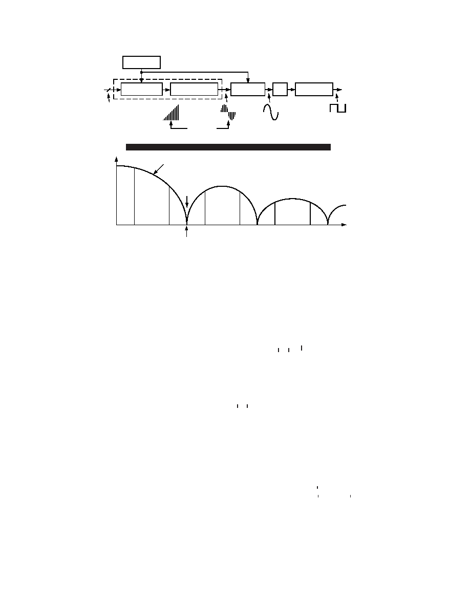
The basic functional block diagram and signal flow of the
AD9851 configured as a clock generator is shown in Figure 11.
The DDS circuitry is basically a digital frequency divider function
whose incremental resolution is determined by the frequency of
the system clock, and N (number of bits in the tuning word). The
phase accumulator is a variable-modulus counter that increments
the number stored in it each time it receives a clock pulse. When
the counter reaches full-scale it wraps around, making the phase
accumulator’s output phase-continuous. The frequency tuning
word sets the modulus of the counter, which effectively determines
the size of the increment ( Phase) that will be added to the value
in the phase accumulator on the next clock pulse. The larger
the added increment, the faster the accumulator wraps around,
which results in a higher output frequency.
The AD9851 uses an innovative and proprietary angle rotation
algorithm that mathematically converts the 14-bit truncated
value of the 32-bit phase accumulator to the 10-bit quantized
amplitude that is passed to the DAC.This unique algorithm uses a
much-reduced ROM look-up table and DSP to perform this func-
tion.This contributes to the small size and low power dissipation of
the AD9851.
The relationship between the output frequency, system clock, and
tuning word of the AD9851 is determined by the expression:
fOUT
ff
= (
OUT
= (
= ( Phase System Clock)/232
where
Phase = decimal value of 32-bit frequency tuning word.
System Clock = direct input reference clock (in MHz) or 6 the
input clock (in MHz) if the 6 REFCLK multiplier is engaged.
fOUT
ff
= frequency of the output signal in MHz.
OUT
The digital sine wave output of the DDS core drives the internal
high speed 10-bit D/A converter that will construct the sine wave
in analog form.This DAC has been optimized for dynamic per-
formance and low glitch energy, which results in the low spurious
and jitter performance of the AD9851.The DAC can be operated
in either the single-ended (Figures 2 and 8) or differential output
configuration (Figures 9 and 10). DAC output current and RSET
values are determined using the following expressions:
IOUT
II
= 39.93/
OUT
RSET
RSET = 39.93/
SET
IOUT
II
Since the output of the AD9851 is a sampled signal, its output
spectrum follows the Nyquist sampling theorem. Specifically,
its output spectrum contains the fundamental plus aliased sig-
nals (images) that occur at integer multiples of the system clock
frequency ± the selected output frequency. A graphical repre-
sentation of the sampled spectrum, with aliased images, is shown
in Figure 12. Normal usable bandwidth is considered to extend
from dc to 1/2 the system clock.
CLOCK
OUT
AMPLITUDE/SINE
CONV ALGORITHM
PHASE
ACCUMULATOR
DDS CIRCUITRY
D/A
CONVERTER
LP
COMPARATOR
N
REFERENCE
CLOCK
TUNING WORD SPECIFIES
OUTPUT FREQUENCY AS A
FRACTION OF REF CLOCK
FREQUENCY
IN DIGITAL
DOMAIN
120MHz
2ND IMAGE
FOUT
FC+FO
2FC–FO
2FC+FO
3FC–FO
180MHz
3RD IMAGE
220MHz
4TH IMAGE
280MHz
5TH IMAGE
80MHz
1ST IMAGE
20MHz
0Hz
(DC)
FC
FC–FO
SIN (X)/ ENVELOPE
= ()F/FC
100MHz
SYSTEM CLOCK FREQUENCY
SIGNAL
AMPLITUDE
Figure 12. Output Spectrum of a Sampled Sin(x)/x Signal
REV. D
相关PDF资料 |
PDF描述 |
|---|---|
| VE-BW3-IY-F3 | CONVERTER MOD DC/DC 24V 50W |
| VE-BW2-IY-F3 | CONVERTER MOD DC/DC 15V 50W |
| AD9850BRSZ-REEL | IC DDS SYNTHESIZER CMOS 28-SSOP |
| VE-BW1-IY-F2 | CONVERTER MOD DC/DC 12V 50W |
| VE-BW0-IY-F2 | CONVERTER MOD DC/DC 5V 50W |
相关代理商/技术参数 |
参数描述 |
|---|---|
| AD9851CGPCB | 制造商:AD 制造商全称:Analog Devices 功能描述:CMOS 180 MHz DDS/DAC Synthesizer |
| AD9851FSPCB | 制造商:Analog Devices 功能描述:EVALUATION BOARD ((NS)) |
| AD9852 | 制造商:AD 制造商全称:Analog Devices 功能描述:CMOS 300 MHz Complete-DDS |
| AD9852/PCB | 制造商:Analog Devices 功能描述:NCO, CMOS 300MSPS COMPLETE-DDS |
| AD9852/PCBZ | 功能描述:BOARD EVAL FOR AD9852 RoHS:是 类别:RF/IF 和 RFID >> RF 评估和开发套件,板 系列:AgileRF™ 标准包装:1 系列:- 类型:GPS 接收器 频率:1575MHz 适用于相关产品:- 已供物品:模块 其它名称:SER3796 |
发布紧急采购,3分钟左右您将得到回复。