参数资料
| 型号: | AD9901KPZ |
| 厂商: | Analog Devices Inc |
| 文件页数: | 4/8页 |
| 文件大小: | 0K |
| 描述: | IC PHS/FREQ DISCRIMINATOR 20PLCC |
| 标准包装: | 49 |
| 类型: | 数字相位/频率鉴别器 |
| PLL: | 是 |
| 输入: | CMOS,ECL,TTL |
| 输出: | CMOS,ECL,TTL |
| 电路数: | 1 |
| 比率 - 输入:输出: | 2:1 |
| 差分 - 输入:输出: | 是/是 |
| 频率 - 最大: | 200MHz |
| 电源电压: | 5V |
| 工作温度: | 0°C ~ 70°C |
| 安装类型: | 表面贴装 |
| 封装/外壳: | 20-LCC(J 形引线) |
| 供应商设备封装: | 20-PLCC(9x9) |
| 包装: | 管件 |
| 产品目录页面: | 551 (CN2011-ZH PDF) |
AD9901
REV. B
–4–
TTL/CMOS MODE FUNCTIONAL PIN DESCRIPTIONS
GROUND
Ground connections for AD9901. Connect
all grounds together and to low impedance
ground plane as close to the device as
possible.
+VS
Positive supply connection; nominally +5.0 V
for TTL operation.
BIAS
Connect to +VS (+5 V) for TTL operation.
VCO INPUT
TTL compatible input; normally connected
to the VCO output signal. VCO INPUT and
REFERENCE INPUT are equivalent to one
another.
OUTPUT
The noninverted output. In TTL/CMOS
mode, the output swing is approximately
+3.2 V to +5 V.
RSET
External RSET connection. The current
through the RSET resistor is equal to the maxi-
mum full-scale output current. RSET should
be connected to ground through an external
resistor in TTL mode. ISET = 0.47 V/RSET =
ILOAD (max).
OUTPUT
The inverted output. In TTL/CMOS mode,
the output swing is approximately +3.2 V to
+5 V.
REFERENCE
TTL compatible input, normally connected
INPUT
to the reference input signal. The VCO
INPUT and the REFERENCE INPUT are
equivalent.
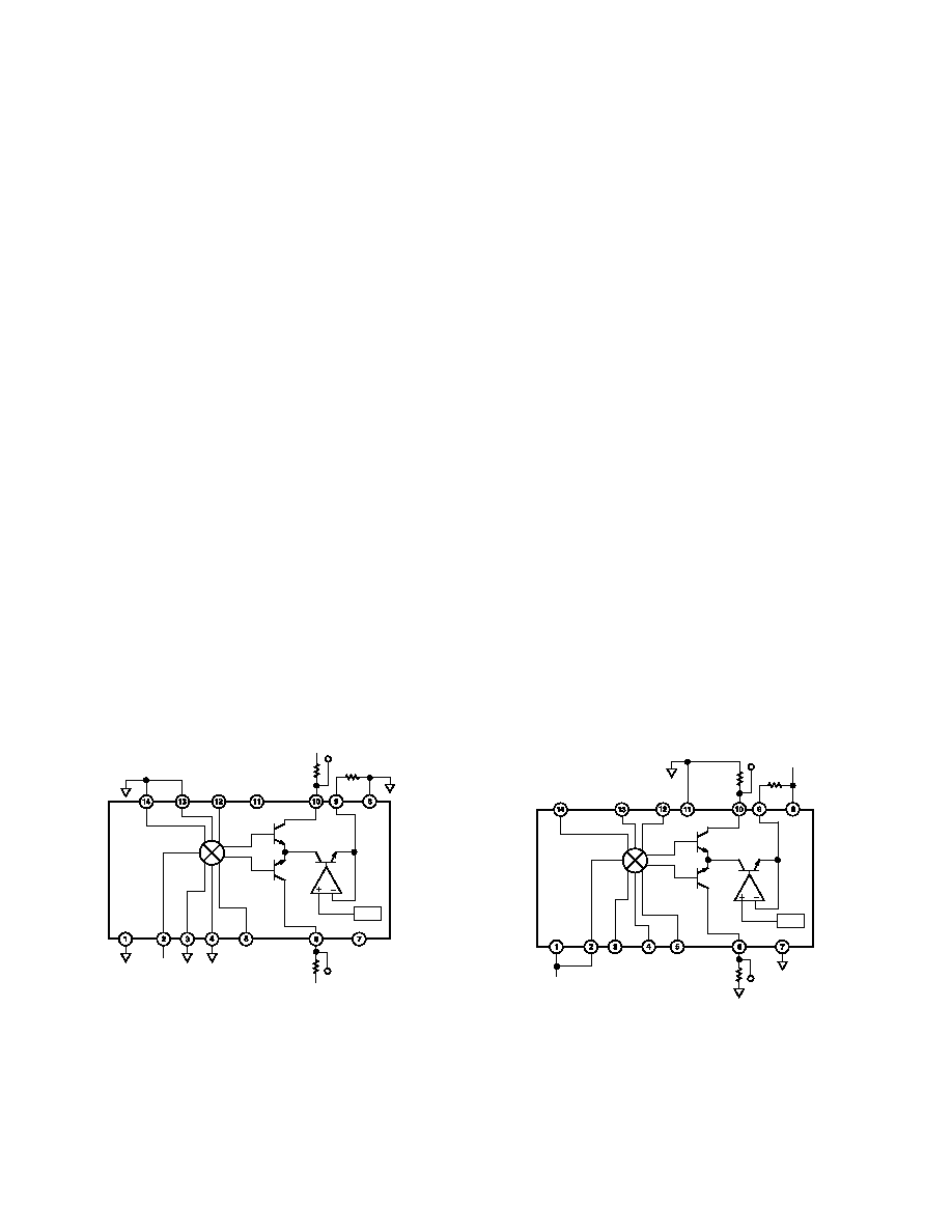
REG
RSET
AD9901
R1
OUTPUT
R2
+VS
REFERENCE
OUTPUT
+VS
VCO
INPUT
BIAS
+VS
R3
Figure 1. TTL Mode (Based on DIP Pinouts)
ECL MODE FUNCTIONAL PIN DESCRIPTIONS
–VS
Negative supply connection, nominally
–5.2 V for ECL operation.
BIAS
Connect to –5.2 V for ECL operation.
VCO INPUT
Inverted side of ECL compatible differential
input, normally connected to the VCO output
signal.
VCO INPUT
Noninverted side of ECL-compatible
differential input, normally connected to the
VCO output signal.
OUTPUT
The noninverted output. In ECL mode, the
output swing is approximately 0 V to –1.8 V.
GROUND
Ground connections for AD9901. Connect
all grounds together and to low-impedance
ground plane as close to the device as
possible.
RSET
External RSET connection. The current
through the RSET resistor is equal to the maxi-
mum full-scale output current. RSET should
be connected to –VS through an external
resistor in ECL mode. ISET = 0.47 V/RSET =
ILOAD (max).
OUTPUT
The inverted output. In ECL mode, the out-
put swing is approximately 0 V to –1.8 V.
REFERENCE
Noninverted side of ECL-compatible
INPUT
differential input, normally connected to the
reference input signal. The VCO INPUT and
the REFERENCE INPUT are equivalent to
one another.
REFERENCE
Inverted side of ECL-compatible differential
INPUT
input, normally connected to the reference
input signal. The
VCO INPUT and the
REFERENCE INPUT are equivalent.
REG
RSET
AD9901
R1
OUTPUT
R2
–VS
REFERENCE
INPUT
OUTPUT
VCO
INPUT
BIAS
R3
REFERENCE
INPUT
–VS
VCO
INPUT
–VS
Figure 2. ECL Mode (Based on DIP Pinouts)
相关PDF资料 |
PDF描述 |
|---|---|
| VE-25P-MX-B1 | CONVERTER MOD DC/DC 13.8V 75W |
| VE-250-MX-B1 | CONVERTER MOD DC/DC 5V 75W |
| ADF4157BRUZ | IC PLL FREQ SYNTH 6GHZ 16TSSOP |
| X9317ZV8Z-2.7 | IC XDCP SGL 100TAP 1K 8-TSSOP |
| CS2200CP-CZZ | IC CLK MULT FRACTIONAL N 10MSOP |
相关代理商/技术参数 |
参数描述 |
|---|---|
| AD9901KPZ | 制造商:Analog Devices 功能描述:IC DISCRIMINATOR ((NW)) |
| AD9901KPZ-REEL | 功能描述:IC DISCRIMINATOR PH/FREQ 20PLCC RoHS:是 类别:集成电路 (IC) >> 时钟/计时 - 时钟发生器,PLL,频率合成器 系列:- 标准包装:1,000 系列:Precision Edge® 类型:时钟/频率合成器 PLL:无 输入:CML,PECL 输出:CML 电路数:1 比率 - 输入:输出:2:1 差分 - 输入:输出:是/是 频率 - 最大:10.7GHz 除法器/乘法器:无/无 电源电压:2.375 V ~ 3.6 V 工作温度:-40°C ~ 85°C 安装类型:表面贴装 封装/外壳:16-VFQFN 裸露焊盘,16-MLF? 供应商设备封装:16-MLF?(3x3) 包装:带卷 (TR) 其它名称:SY58052UMGTRSY58052UMGTR-ND |
| AD9901KQ | 功能描述:IC PHASE/FREQ DISCRIMR 14-CDIP RoHS:否 类别:集成电路 (IC) >> 时钟/计时 - 时钟发生器,PLL,频率合成器 系列:- 标准包装:2,000 系列:- 类型:PLL 时钟发生器 PLL:带旁路 输入:LVCMOS,LVPECL 输出:LVCMOS 电路数:1 比率 - 输入:输出:2:11 差分 - 输入:输出:是/无 频率 - 最大:240MHz 除法器/乘法器:是/无 电源电压:3.135 V ~ 3.465 V 工作温度:0°C ~ 70°C 安装类型:表面贴装 封装/外壳:32-LQFP 供应商设备封装:32-TQFP(7x7) 包装:带卷 (TR) |
| AD9901TE/883 | 制造商:AD 制造商全称:Analog Devices 功能描述:Ultrahigh Speed Phase/Frequency Discriminator |
| AD9901TQ/883 | 制造商:AD 制造商全称:Analog Devices 功能描述:Ultrahigh Speed Phase/Frequency Discriminator |
发布紧急采购,3分钟左右您将得到回复。