参数资料
| 型号: | AD9901KPZ |
| 厂商: | Analog Devices Inc |
| 文件页数: | 6/8页 |
| 文件大小: | 0K |
| 描述: | IC PHS/FREQ DISCRIMINATOR 20PLCC |
| 标准包装: | 49 |
| 类型: | 数字相位/频率鉴别器 |
| PLL: | 是 |
| 输入: | CMOS,ECL,TTL |
| 输出: | CMOS,ECL,TTL |
| 电路数: | 1 |
| 比率 - 输入:输出: | 2:1 |
| 差分 - 输入:输出: | 是/是 |
| 频率 - 最大: | 200MHz |
| 电源电压: | 5V |
| 工作温度: | 0°C ~ 70°C |
| 安装类型: | 表面贴装 |
| 封装/外壳: | 20-LCC(J 形引线) |
| 供应商设备封装: | 20-PLCC(9x9) |
| 包装: | 管件 |
| 产品目录页面: | 551 (CN2011-ZH PDF) |
AD9901
REV. B
–6–
THEORY OF OPERATION
A phase detector is one of three basic components of a phase-
locked loop (PLL); the other two are a filter and a tunable oscil-
lator. A basic PLL control system is shown in Figure 3.
LOW-
PASS
FILTER
1/N
VCO
AD9901
REFERENCE
INPUT
OSCILLATOR
OUTPUT
OPTIONAL 1/N PRESCALER
TYPICAL OF DIGITAL PLLs
Figure 3. Phase-Locked Loop Control System
The function of the phase detector is to generate an error signal
that is used to retune the oscillator frequency whenever its out-
put deviates from a reference input signal. The two most com-
mon methods of implementing phase detectors are (1) an analog
mixer and (2) a family of sequential logic circuits known as
digital phase detectors.
The AD9901 is a digital phase detector. As illustrated in the
block diagram of the unit, straightforward sequential logic de-
sign is used. The main components include four “D” flip-flops,
an exclusive-OR gate (XOR) and some combinational output
logic. The circuit operates in two distinct modes: as a linear
phase detector and as a frequency discriminator.
When the reference and oscillator are very close in frequency,
only the phase detection circuit is active. If the two inputs are
substantially different in frequency, the frequency discrimina-
tion circuit overrides the phase detector portion to drive the
oscillator frequency toward the reference frequency and put it
within range of the phase detector.
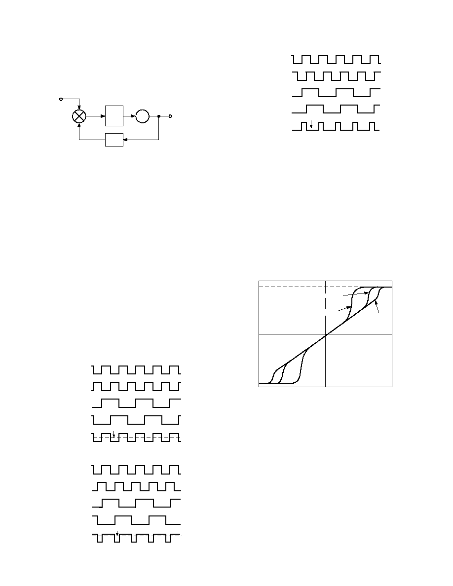
Input signals to the AD9901 are pulse trains, and its output
duty cycle is proportional to the phase difference of the oscilla-
tor and reference inputs. Figures 4, 5 and 6 illustrate, respec-
tively, the input/output relationships at lock; with the
DC MEAN VALUE
REFERENCE
INPUT
OSCILLATOR
INPUT
REFERENCE
FLIP-FLOP
OUTPUT
OSCILLATOR
FLIP-FLOP
OUTPUT
XORGATE
OUTPUT
Figure 4. AD9901 Timing Waveforms at “Lock”
DC MEAN VALUE
REFERENCE
INPUT
OSCILLATOR
INPUT
REFERENCE
FLIP-FLOP
OUTPUT
OSCILLATOR
FLIP-FLOP
OUTPUT
XORGATE
OUTPUT
Figure 5. Timing Waveforms (
φ
OUT Leads φIN)
DC MEAN VALUE
REFERENCE
INPUT
OSCILLATOR
INPUT
REFERENCE
FLIP-FLOP
OUTPUT
OSCILLATOR
FLIP-FLOP
OUTPUT
XORGATE
OUTPUT
Figure 6. Timing Waveforms (
φ
OUT Lags φIN)
oscillator leading the reference frequency; and with the oscillator
lagging. This output pulse train is low-pass filtered to extract the
dc mean value [Kφ (φI – φO)] where Kφ is a proportionality con-
stant (phase gain).
At or near lock (Figures 4, 5 and 6), only the two input flip-
flops and the exclusive-OR gate (the phase detection circuit) are
active. The input flip-flops divide both the reference and oscilla-
tor frequencies by a factor of two. This insures that inputs to the
exclusive-OR are square waves, regardless of the input duty
cycles of the frequencies being compared. This division-by-two
also moves the nonlinear detection range to the ends of the
range rather than near lock, which is the case with conventional
digital phase detectors.
Figure 7 illustrates the constant gain near lock.
PHASE DIFFERENCE AT INPUTS
2
1
0
–2
0
OUTPUT
VOLTAGE
SWING
–
FO = 50MHz
FO = 70MHz
FO = 200MHz
TYPICAL PHASE DETECTOR
GAIN IS 0.2865V/RAD
VOUT = 1.8V
Figure 7. Phase Gain Plot
When the two square waves are combined by the XOR, the
output has a 50% duty cycle if the reference and oscillator in-
puts are exactly 180
° out of phase; under these conditions, the
AD9901 is operating in a locked mode. Any shift in the phase
relationship between these input signals causes a change in the
output duty cycle. Near lock, the frequency discriminator flip-
flops provide constant HIGH levels to gate the XOR output to
the final output.
The duty cycle of the AD9901 is a direct measure of the phase
difference between the two input signals when the unit is near
lock. The transfer function can be stated as [Kφ(φI – φO](V/RAD),
where Kφ is the allowable output voltage range of the AD9901
divided by 2
π.
For a typical output swing of 1.8 V, the transfer function can be
stated as (1.8 V/2
π = 0.285 V/RAD). Figure 7 shows the rela-
tionship of the dc mean value of the AD9901 output as a func-
tion of the phase difference of the two inputs.
相关PDF资料 |
PDF描述 |
|---|---|
| VE-25P-MX-B1 | CONVERTER MOD DC/DC 13.8V 75W |
| VE-250-MX-B1 | CONVERTER MOD DC/DC 5V 75W |
| ADF4157BRUZ | IC PLL FREQ SYNTH 6GHZ 16TSSOP |
| X9317ZV8Z-2.7 | IC XDCP SGL 100TAP 1K 8-TSSOP |
| CS2200CP-CZZ | IC CLK MULT FRACTIONAL N 10MSOP |
相关代理商/技术参数 |
参数描述 |
|---|---|
| AD9901KPZ | 制造商:Analog Devices 功能描述:IC DISCRIMINATOR ((NW)) |
| AD9901KPZ-REEL | 功能描述:IC DISCRIMINATOR PH/FREQ 20PLCC RoHS:是 类别:集成电路 (IC) >> 时钟/计时 - 时钟发生器,PLL,频率合成器 系列:- 标准包装:1,000 系列:Precision Edge® 类型:时钟/频率合成器 PLL:无 输入:CML,PECL 输出:CML 电路数:1 比率 - 输入:输出:2:1 差分 - 输入:输出:是/是 频率 - 最大:10.7GHz 除法器/乘法器:无/无 电源电压:2.375 V ~ 3.6 V 工作温度:-40°C ~ 85°C 安装类型:表面贴装 封装/外壳:16-VFQFN 裸露焊盘,16-MLF? 供应商设备封装:16-MLF?(3x3) 包装:带卷 (TR) 其它名称:SY58052UMGTRSY58052UMGTR-ND |
| AD9901KQ | 功能描述:IC PHASE/FREQ DISCRIMR 14-CDIP RoHS:否 类别:集成电路 (IC) >> 时钟/计时 - 时钟发生器,PLL,频率合成器 系列:- 标准包装:2,000 系列:- 类型:PLL 时钟发生器 PLL:带旁路 输入:LVCMOS,LVPECL 输出:LVCMOS 电路数:1 比率 - 输入:输出:2:11 差分 - 输入:输出:是/无 频率 - 最大:240MHz 除法器/乘法器:是/无 电源电压:3.135 V ~ 3.465 V 工作温度:0°C ~ 70°C 安装类型:表面贴装 封装/外壳:32-LQFP 供应商设备封装:32-TQFP(7x7) 包装:带卷 (TR) |
| AD9901TE/883 | 制造商:AD 制造商全称:Analog Devices 功能描述:Ultrahigh Speed Phase/Frequency Discriminator |
| AD9901TQ/883 | 制造商:AD 制造商全称:Analog Devices 功能描述:Ultrahigh Speed Phase/Frequency Discriminator |
发布紧急采购,3分钟左右您将得到回复。