- 您现在的位置:买卖IC网 > PDF目录16458 > AD9911/PCBZ (Analog Devices Inc)BOARD EVAL FOR AD9911 PDF资料下载
参数资料
| 型号: | AD9911/PCBZ |
| 厂商: | Analog Devices Inc |
| 文件页数: | 26/44页 |
| 文件大小: | 0K |
| 描述: | BOARD EVAL FOR AD9911 |
| 产品培训模块: | Direct Digital Synthesis Tutorial Series (1 of 7): Introduction Direct Digital Synthesizer Tutorial Series (7 of 7): DDS in Action Direct Digital Synthesis Tutorial Series (3 of 7): Angle to Amplitude Converter Direct Digital Synthesis Tutorial Series (6 of 7): SINC Envelope Correction Direct Digital Synthesis Tutorial Series (4 of 7): Digital-to-Analog Converter Direct Digital Synthesis Tutorial Series (2 of 7): The Accumulator |
| 设计资源: | AD9911 Eval Brd Schematics AD9911 Eval Brd BOM AD9911 Eval Brd Gerber Files |
| 标准包装: | 1 |
| 系列: | AgileRF™ |
| 主要目的: | 计时,直接数字合成(DDS) |
| 已用 IC / 零件: | AD9911 |
| 已供物品: | 板 |
| 相关产品: | AD9911BCPZ-REEL7-ND - IC DDS 500MSPS DAC 10BIT 56LFCSP AD9911BCPZ-ND - IC DDS 500MSPS DAC 10BIT 56LFCSP |
第1页第2页第3页第4页第5页第6页第7页第8页第9页第10页第11页第12页第13页第14页第15页第16页第17页第18页第19页第20页第21页第22页第23页第24页第25页当前第26页第27页第28页第29页第30页第31页第32页第33页第34页第35页第36页第37页第38页第39页第40页第41页第42页第43页第44页
AD9911
Rev. 0 | Page 32 of 44
Single-Bit Serial (2- and 3-Wire) Modes
The single-bit serial mode interface allows read/write access to
all registers that configure the AD9911. MSB-first or LSB-first
transfer formats and the SYNC_I/O function are supported.
In 2-wire mode, the SDIO_0 pin is the single serial data I/O pin.
In 3-wire mode, the SDIO_0 pin is the serial data input pin and
the SDIO_2 pin is the output. For both modes, the SDIO_3 pin
is configured as an input and operates as the SYNC_I/O pin.
The SDIO_1 pin is unused.
2-Bit Mode
The SPI port operation in 2-bit mode is identical to the SPI port
operation in single bit mode, except that two bits of data are
registered on each rising edge of SCLK, cutting in half the
number of cycles required to program the device. The SDIO_0
pin contains the even numbered data bits using the notation D
<7:0> while the SDIO_1 pin contains the odd numbered data
bits regardless of whether in MSB- or LSB-first format (see
4-Bit Mode
The SPI port in 4-bit mode is identical to the SPI port in single
bit mode, except that four bits of data are registered on each
rising edge of SCLK.
This reduces by 75% the number of cycles required to program
the device. Note that when reprogramming the device for 4-bit
mode, it is important to keep the SDIO_3 pin at Logic 0 until
the device is programmed out of the single bit serial mode.
Failure to do so can result in the I/O port controller being out of
sequence.
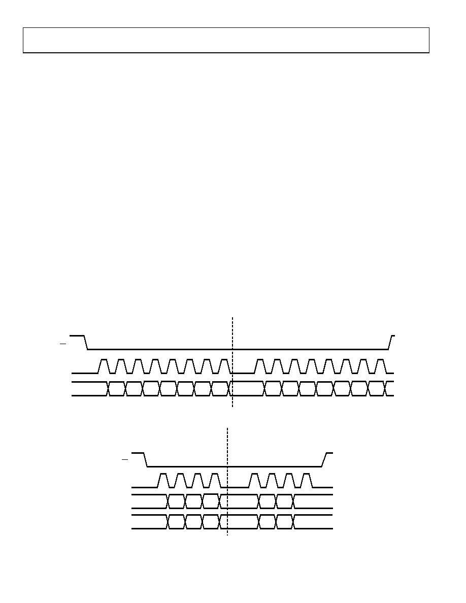
I/O modes available. Both MSB and LSB-first modes are shown.
LSB-first bits are shown in parenthesis. The clock stall low/high
feature shown is not required, but rather is used to show that
data (SDIO) must have the proper setup time relative to the
rising edge of SCLK.
I/O mode available. Both MSB and LSB-first modes are shown.
LSB-first bits are shown in parenthesis. The clock stall low/high
feature shown is not required. It is used to show that data
(SDIO) must have the proper set-up time relative to the rising
edge of SCLK for the instruction byte and the read data that
follows the falling edge of SCLK.
SCLK
SDIO_0
INSTRUCTION CYCLE
DATA TRANSFER CYCLE
CS
I7
(I0)
I6
(I1)
I5
(I2)
I4
(I3)
I3
(I4)
I2
(I5)
I1
(I6)
I0
(I7)
D7
(D0)
D6
(D1)
D5
(D2)
D4
(D3)
D3
(D4)
D2
(D5)
D1
(D6)
D0
(D7)
05
78
5-
04
7
Figure 50. Single-Bit Serial Mode Write Timing—Clock Stall Low
INSTRUCTION CYCLE
DATA TRANSFER CYCLE
CS
SCLK
SDIO_1
SDIO_0
D7
(D1)
D5
(D3)
D3
(D5)
D1
(D7)
D6
(D0)
D4
(D2)
D2
(D4)
D0
(D6)
I6
(I0)
I4
(I2)
I2
(I4)
I0
(I6)
I7
(I1)
I5
(I3)
I3
(I5)
I1
(I7)
05
78
5-
0
48
Figure 51. 2-Bit Mode Write Timing—Clock Stall Low
相关PDF资料 |
PDF描述 |
|---|---|
| CM252016-33NKL | INDUCTOR CHIP .033UH 2520 SMD |
| VE-24M-EX | CONVERTER MOD DC/DC 10V 75W |
| 2-5504971-0 | CA 62.5/125 LDDZP SCDUP-SCDUP |
| LK2125R82K-T | INDUCTOR MULTILAYER .82UH 0805 |
| UPM1E122MHD6TN | CAP ALUM 1200UF 25V 20% RADIAL |
相关代理商/技术参数 |
参数描述 |
|---|---|
| AD9912 | 制造商:AD 制造商全称:Analog Devices 功能描述:1 GSPS Direct Digital Synthesizer w/ 14-bit DAC |
| AD9912/PCBZ | 制造商:Analog Devices 功能描述:Evaluation Kit For 1 GSPS Direct Digital Synthesizer W/ 14-Bit DAC 制造商:Analog Devices 功能描述:EVAL KIT FOR 1 GSPS DIRECT DGTL SYNTHESIZER W/ 14BIT DAC - Bulk 制造商:Analog Devices 功能描述:EVALUATION BOARD AD9912 1GSPS DDS |
| AD9912A/PCBZ | 功能描述:BOARD EVALUATION FOR AD9912 RoHS:是 类别:编程器,开发系统 >> 评估演示板和套件 系列:- 标准包装:1 系列:PCI Express® (PCIe) 主要目的:接口,收发器,PCI Express 嵌入式:- 已用 IC / 零件:DS80PCI800 主要属性:- 次要属性:- 已供物品:板 |
| AD9912ABCPZ | 功能描述:IC DDS 1GSPS DAC 14BIT 64LFCSP RoHS:是 类别:集成电路 (IC) >> 接口 - 直接数字合成 (DDS) 系列:- 产品变化通告:Product Discontinuance 27/Oct/2011 标准包装:2,500 系列:- 分辨率(位):10 b 主 fclk:25MHz 调节字宽(位):32 b 电源电压:2.97 V ~ 5.5 V 工作温度:-40°C ~ 85°C 安装类型:表面贴装 封装/外壳:16-TSSOP(0.173",4.40mm 宽) 供应商设备封装:16-TSSOP 包装:带卷 (TR) |
| AD9912ABCPZ-REEL7 | 功能描述:IC DDS 1GSPS DAC 14BIT 64LFCSP RoHS:是 类别:集成电路 (IC) >> 接口 - 直接数字合成 (DDS) 系列:- 产品变化通告:Product Discontinuance 27/Oct/2011 标准包装:2,500 系列:- 分辨率(位):10 b 主 fclk:25MHz 调节字宽(位):32 b 电源电压:2.97 V ~ 5.5 V 工作温度:-40°C ~ 85°C 安装类型:表面贴装 封装/外壳:16-TSSOP(0.173",4.40mm 宽) 供应商设备封装:16-TSSOP 包装:带卷 (TR) |
发布紧急采购,3分钟左右您将得到回复。