- 您现在的位置:买卖IC网 > PDF目录10979 > AD9956YCPZ (Analog Devices Inc)IC SYNTHESIZER 1.8V 48LFCSP PDF资料下载
参数资料
| 型号: | AD9956YCPZ |
| 厂商: | Analog Devices Inc |
| 文件页数: | 16/32页 |
| 文件大小: | 0K |
| 描述: | IC SYNTHESIZER 1.8V 48LFCSP |
| 产品培训模块: | Direct Digital Synthesis Tutorial Series (1 of 7): Introduction Direct Digital Synthesizer Tutorial Series (7 of 7): DDS in Action Direct Digital Synthesis Tutorial Series (3 of 7): Angle to Amplitude Converter Direct Digital Synthesis Tutorial Series (6 of 7): SINC Envelope Correction Direct Digital Synthesis Tutorial Series (4 of 7): Digital-to-Analog Converter Direct Digital Synthesis Tutorial Series (2 of 7): The Accumulator |
| 标准包装: | 1 |
| 分辨率(位): | 14 b |
| 主 fclk: | 3GHz |
| 调节字宽(位): | 48 b |
| 电源电压: | 1.71 V ~ 1.96 V |
| 工作温度: | -40°C ~ 125°C |
| 安装类型: | 表面贴装 |
| 封装/外壳: | 48-VFQFN 裸露焊盘,CSP |
| 供应商设备封装: | 48-LFCSP-VQ(7x7) |
| 包装: | 托盘 |
| 产品目录页面: | 552 (CN2011-ZH PDF) |
| 配用: | AD9956-VCO/PCBZ-ND - BOARD EVAL 14BIT 1.8V 48LFCSP AD9956/PCBZ-ND - BOARD EVAL FOR AD9956 |
第1页第2页第3页第4页第5页第6页第7页第8页第9页第10页第11页第12页第13页第14页第15页当前第16页第17页第18页第19页第20页第21页第22页第23页第24页第25页第26页第27页第28页第29页第30页第31页第32页
AD9956
Rev. A | Page 23 of 32
INSTRUCTION BYTE
The instruction byte contains the following information:
Table 4.
D7
D6
D5
D4
D3
D2
D1
D0
R/Wb
X
A4
A3
A2
A1
A0
R/Wb—Bit 7 of the instruction byte determines whether a read
or write data transfer occurs after the instruction byte write.
Logic 1 indicates a read operation. Logic 0 indicates a write
operation.
X, X—Bits 6 and 5 of the instruction byte are Don’t Care.
A4 to A0—Bits 4 to 0 of the instruction byte determine which
register is accessed during the data transfer portion of the
communications cycle.
SERIAL INTERFACE PORT PIN DESCRIPTION
SCLK—Serial Clock. The serial clock pin is used to synchronize
data to and from the AD9956 and to run the internal state
machines. The SCLK maximum frequency is 25 MHz.
CS—Chip Select Bar. CS is an active low input that allows more
than one device on the same serial communications line. The
SDO and SDI/O pins go to a high impedance state when this
input is high. If driven high during any communications cycle,
that cycle is suspended until CS is reactivated low. Chip select
can be tied low in systems that maintain control of SCLK.
SDI/O—Serial Data Input/Output. Data is always written to the
AD9956 on this pin. However, this pin can be used as a bidirec-
tional data line. CFR1<7> controls the configuration of this pin.
The default value (0) configures the SDI/O pin as bidirectional.
SDO—Serial Data Out. Data is read from this pin for protocols
that use separate lines for transmitting and receiving data. When
the AD9956 operates in a single bidirectional I/O mode, this pin
does not output data and is set to a high impedance state.
I/O_RESET—A high signal on this pin resets the I/O port state
machines without affecting the addressable registers’ contents.
An active high input on the I/O_RESET pin causes the current
communication cycle to abort. After I/O_RESET returns low
(0), another communication cycle can begin, starting with the
instruction byte write. Note that when not in use, this pin
should be forced low, because it floats to the threshold value.
MSB/LSB TRANSFERS
The AD9956 serial port can support both most significant bit
(MSB) first or least significant bit (LSB) first data formats. This
functionality is controlled by the LSB first bit in Control
Register 1 (CFR1<15>). The default value of this bit is low
(MSB first). When CFR1 <15> is set high, the AD9956 serial
port is in LSB first format. The instruction byte must be written
in the format indicated by CFR1 <15>. If the AD9956 is in LSB
first mode, the instruction byte must be written from least
significant bit to most significant bit. However, the instruction
byte phase of the communications cycle still precedes the data
transfer cycle.
For MSB first operation, all data written to (read from) the
AD9956 are in MSB first order. If the LSB mode is active, all
data written to (read from) the AD9956 are in LSB first order.
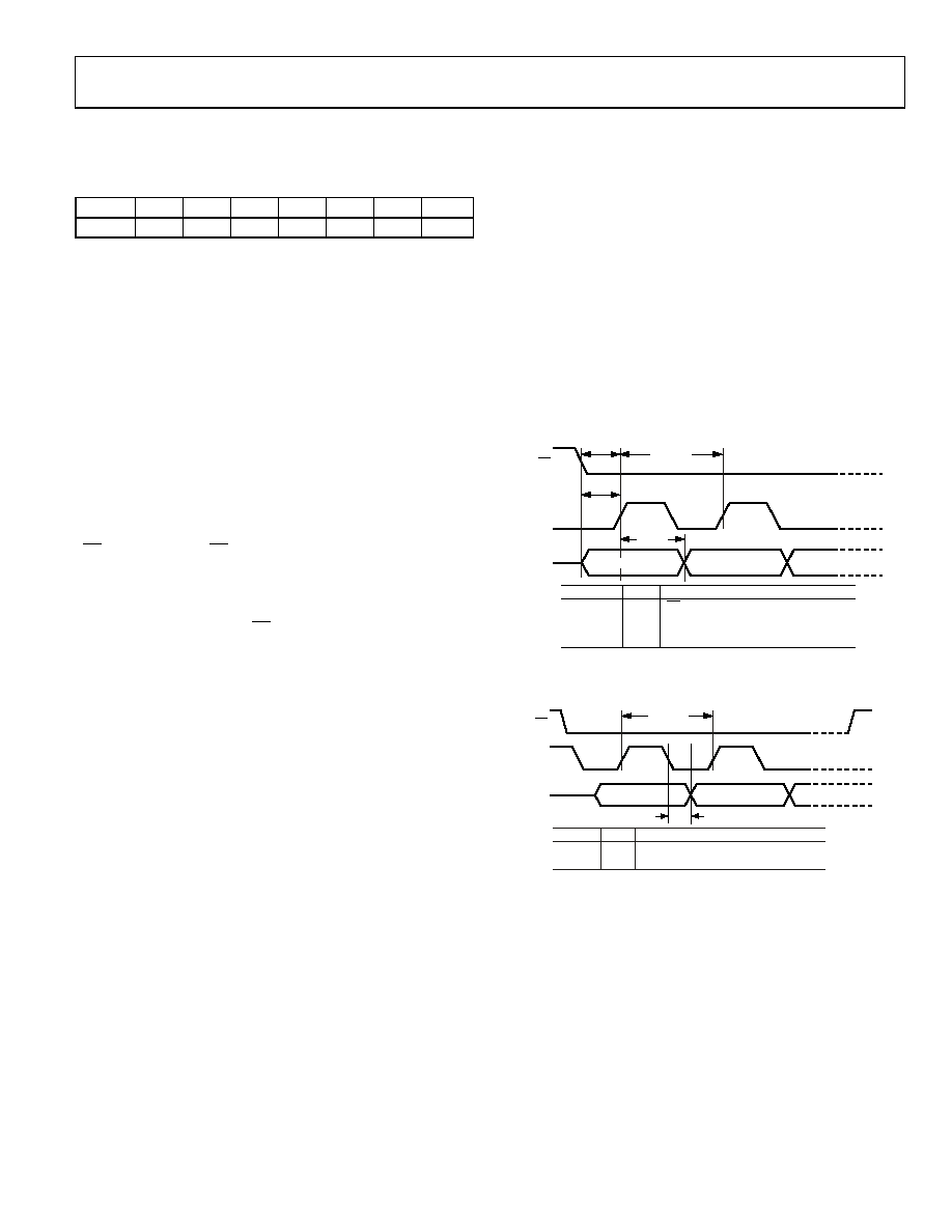
CS
SCLK
SDI/O
TPRE
TDSU
TSCLKW
TDHLD
SECOND BIT
FIRST BIT
SYMBOL
TPRE
TSCLKW
TDSU
TDHLD
MIN
6ns
40ns
6.5ns
0ns
DEFINITION
CS SETUP TIME
PERIOD OF SERIAL DATA CLOCK (WRITE)
SERIAL DATA SETUP TIME
SERIAL DATA HOLD TIME
04806-0-034
Figure 33. Timing Diagram for Data Write to AD9956
TDV
FIRST BIT
SECOND BIT
SDI/O
SDO
SCLK
CS
SYMBOL
TDV
TSCLKR
MAX
40ns
400ns
DEFINITION
DATA VALID TIME
PERIOD OF SERIAL DATA CLOCK (READ)
04806-0-035
TSCLKR
Figure 34. Timing Diagram for Data Read to AD9956
相关PDF资料 |
PDF描述 |
|---|---|
| S9S08DZ60F1MLH | MCU 60K FLASH MASK AUTO 64-LQFP |
| AD9952YSVZ | IC DDS 14BIT DAC 1.8V 48-TQFP |
| MC9S08DZ96MLF | MCU 8BIT 96K FLASH 48-LQFP |
| AD5933YRSZ | IC NTWK ANALYZER 12B 1MSP 16SSOP |
| MC908JL3EMPE | IC MCU 4K FLASH W/OSC 28-PDIP |
相关代理商/技术参数 |
参数描述 |
|---|---|
| AD9956YCPZ1 | 制造商:AD 制造商全称:Analog Devices 功能描述:2.7 GHz DDS-Based AgileRF |
| AD9956YCPZ-REEL1 | 制造商:AD 制造商全称:Analog Devices 功能描述:2.7 GHz DDS-Based AgileRF |
| AD9956YCPZ-REEL7 | 功能描述:IC SYNTHESIZER 1.8V 48LFCSP RoHS:是 类别:集成电路 (IC) >> 接口 - 直接数字合成 (DDS) 系列:- 产品变化通告:Product Discontinuance 27/Oct/2011 标准包装:2,500 系列:- 分辨率(位):10 b 主 fclk:25MHz 调节字宽(位):32 b 电源电压:2.97 V ~ 5.5 V 工作温度:-40°C ~ 85°C 安装类型:表面贴装 封装/外壳:16-TSSOP(0.173",4.40mm 宽) 供应商设备封装:16-TSSOP 包装:带卷 (TR) |
| AD9957 | 制造商:AD 制造商全称:Analog Devices 功能描述:1 GSPS Quadrature Digital Upconverter with 18-Bit IQ Data Path and 14-Bit DAC |
| AD9957/PCBZ | 功能描述:BOARD EVAL AD9957 QUADRATURE MOD RoHS:是 类别:编程器,开发系统 >> 评估演示板和套件 系列:AgileRF™ 标准包装:1 系列:PSoC® 主要目的:电源管理,热管理 嵌入式:- 已用 IC / 零件:- 主要属性:- 次要属性:- 已供物品:板,CD,电源 |
发布紧急采购,3分钟左右您将得到回复。