- 您现在的位置:买卖IC网 > PDF目录11769 > AD9980KSTZ-80 (Analog Devices Inc)IC INTERFACE 8BIT ANALOG 80LQFP PDF资料下载
参数资料
| 型号: | AD9980KSTZ-80 |
| 厂商: | Analog Devices Inc |
| 文件页数: | 2/44页 |
| 文件大小: | 0K |
| 描述: | IC INTERFACE 8BIT ANALOG 80LQFP |
| 标准包装: | 90 |
| 应用: | 视频 |
| 接口: | 模拟 |
| 电源电压: | 3.13 V ~ 3.47 V |
| 封装/外壳: | 80-LQFP |
| 供应商设备封装: | 80-LQFP(14x14) |
| 包装: | 管件 |
| 安装类型: | 表面贴装 |
| 配用: | AD9980/PCBZ-ND - KIT EVALUATION AD9980 |
第1页当前第2页第3页第4页第5页第6页第7页第8页第9页第10页第11页第12页第13页第14页第15页第16页第17页第18页第19页第20页第21页第22页第23页第24页第25页第26页第27页第28页第29页第30页第31页第32页第33页第34页第35页第36页第37页第38页第39页第40页第41页第42页第43页第44页
AD9980
Rev. 0 | Page 10 of 44
DESIGN GUIDE
GENERAL DESCRIPTION
The AD9980 is a fully integrated solution for capturing analog
RGB or YPbPr signals and digitizing them for display on
advanced TVs, flat panel monitors, projectors, and other types
of digital displays. Implemented in a high-performance CMOS
process, the interface can capture signals with pixel rates of up
to 95 MHz.
The AD9980 includes all necessary input buffering, signal dc
restoration (clamping), offset and gain (brightness and contrast)
adjustment, pixel clock generation, sampling phase control, and
output data formatting. All controls are programmable via a
two-wire serial interface (I2C
). Full integration of these
sensitive analog functions makes system design straightforward
and less sensitive to the physical and electrical environment.
With a typical power dissipation of less than 900 mW and an
operating temperature range of 0°C to 70°C, the device requires
no special environmental considerations.
DIGITAL INPUTS
All digital inputs on the AD9980 operate to 3.3 V CMOS levels.
The following digital inputs are 5 V tolerant (Applying 5 V to
them does not cause any damage): HSYNC0, HSYNC1,
VSYNC0, VSYNC1, SOGIN0, SOGIN1, SDA, SCL and CLAMP.
INPUT SIGNAL HANDLING
The AD9980 has six high-impedance analog input pins for the
red, green, and blue channels. They accommodate signals
ranging from 0.5 V to 1.0 V p-p.
Signals are typically brought onto the interface board with a
DVI-I connector, a 15-pin D connector, or RCA connectors.
The AD9980 should be located as close as possible to the input
connector. Signals should be routed using matched-impedance
traces (normally 75 ) to the IC input pins.
At the input pins the signal should be resistively terminated
(75 to the signal ground return) and capacitively coupled to
the AD9980 inputs through 47 nF capacitors. These capacitors
form part of the dc restoration circuit.
In an ideal world of perfectly matched impedances, the best
performance can be obtained with the widest possible signal
bandwidth. The wide bandwidth inputs of the AD9980
(200 MHz) can continuously track the input signal as it moves
from one pixel level to the next and can digitize the pixel during
a long, flat pixel time. In many systems, however, there are mis-
matches, reflections, and noise, which can result in excessive
ringing and distortion of the input waveform. This makes it
more difficult to establish a sampling phase that provides good
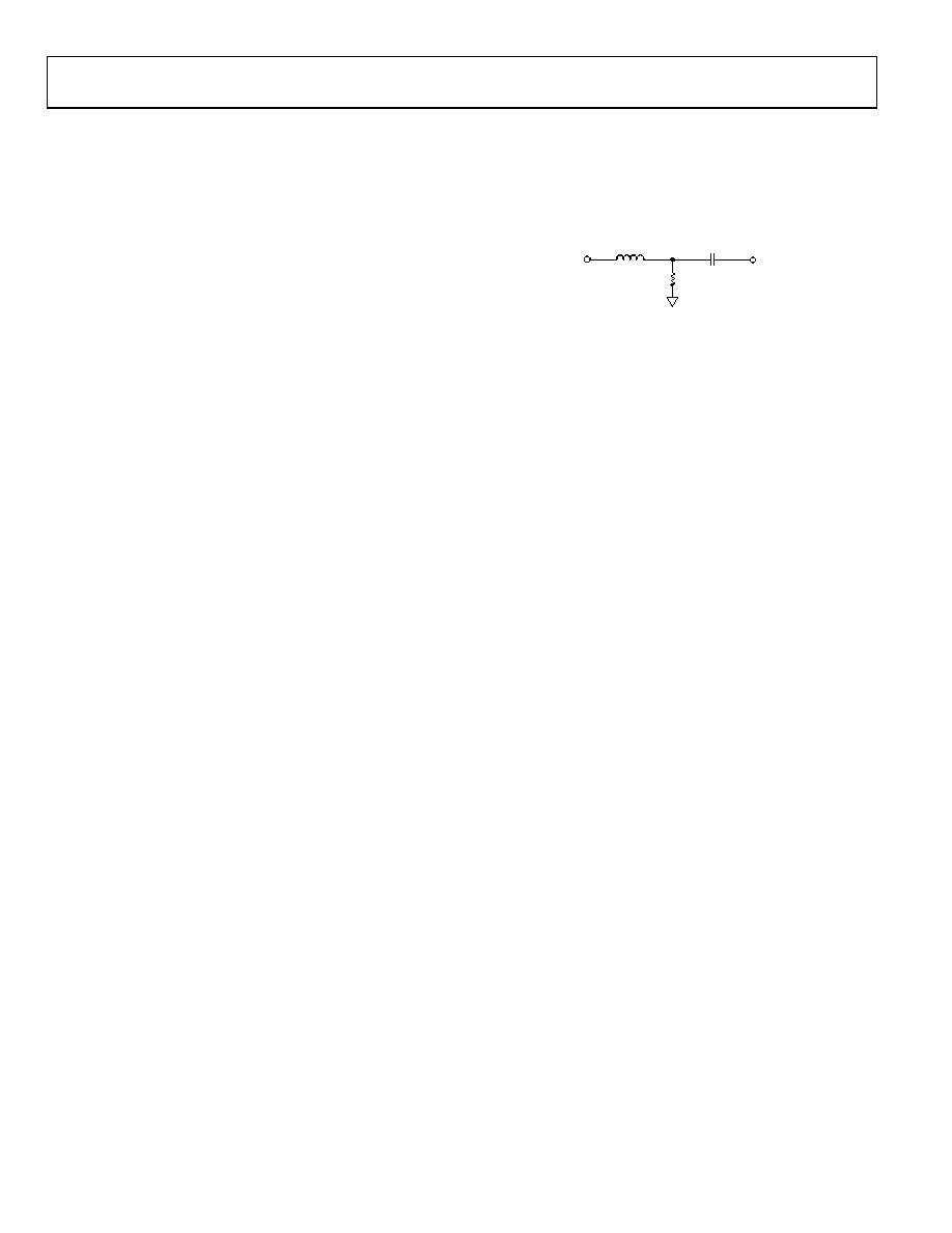
image quality. It has been shown that a small inductor in series
with the input is effective in rolling off the input bandwidth
slightly and providing a high quality signal over a wider range
of conditions. Using a Fair-Rite #2508051217Z0 high speed,
signal chip bead inductor in the circuit shown in Figure 3 gives
good results in most applications.
RGB
INPUT
RAIN
GAIN
BAIN
47nF
75
04740-002
Figure 3. Analog Input Interface Circuit
HSYNC AND VSYNC INPUTS
The interface also accepts Hsync and vertical sync period
(Vsync) signals, which are used to generate the pixel clock,
clamp timing, Coast and field information. These can be either
a sync signal directly from the graphics source, or a
preprocessed TTL or CMOS level signal.
The Hsync input includes a Schmitt trigger buffer for immunity
to noise and signals with long rise times. In typical PC-based
graphic systems, the sync signals are simply TTL-level drivers
feeding unshielded wires in the monitor cable. As such, no
termination is required.
SERIAL CONTROL PORT
The serial control port is designed for 3.3 V logic; however, it is
tolerant of 5 V logic signals.
OUTPUT SIGNAL HANDLING
The digital outputs are designed to operate from 1.8 V to
3.3 V (VDD).
CLAMPING
RGB Clamping
To properly digitize the incoming signal, the dc offset of the
input must be adjusted to fit the range of the on-board ADCs.
Most graphics systems produce RGB signals with black at
ground and white at approximately 0.75 V. However, if sync
signals are embedded in the graphics, the sync tip is often at
ground and black is at 300 mV. Then white is at approximately
1.0 V. Some common RGB line amplifier boxes use emitter-
follower buffers to split signals and increase drive capability.
This introduces a 700 mV dc offset to the signal, which must be
removed for proper capture by the AD9980.
The key to clamping is to identify a portion (time) of the signal
when the graphic system is known to be producing black. An
offset is then introduced that results in the ADCs producing a
black output (Code 0x00) when the known black input is
present. The offset then remains in place when other signal
levels are processed, and the entire signal is shifted to eliminate
offset errors.
相关PDF资料 |
PDF描述 |
|---|---|
| V150B24H150BL | CONVERTER MOD DC/DC 24V 150W |
| SY100E445JZ TR | IC CONV 4BIT SER/PAR 28-PLCC |
| SY10E446JZ TR | IC CONV 4BIT PAR/SER 28-PLCC |
| SY10E445JZ TR | IC CONV 4BIT SER/PAR 28-PLCC |
| D38999/26FC8SN | CONN PLUG 8POS STRAIGHT W/SCKT |
相关代理商/技术参数 |
参数描述 |
|---|---|
| AD9980KSTZ-95 | 功能描述:IC INTERFACE 8BIT ANALOG 80LQFP RoHS:是 类别:集成电路 (IC) >> 接口 - 专用 系列:- 特色产品:NXP - I2C Interface 标准包装:1 系列:- 应用:2 通道 I²C 多路复用器 接口:I²C,SM 总线 电源电压:2.3 V ~ 5.5 V 封装/外壳:16-TSSOP(0.173",4.40mm 宽) 供应商设备封装:16-TSSOP 包装:剪切带 (CT) 安装类型:表面贴装 产品目录页面:825 (CN2011-ZH PDF) 其它名称:568-1854-1 |
| AD9980KSTZ-RL95 | 制造商:Analog Devices 功能描述: |
| AD9980PCB | 制造商:AD 制造商全称:Analog Devices 功能描述:High Performance 8-Bit Display Interface |
| AD9981 | 制造商:AD 制造商全称:Analog Devices 功能描述:High Performance 10-Bit Display Interface |
| AD9981/PCB | 制造商:AD 制造商全称:Analog Devices 功能描述:High Performance 10-Bit Display Interface |
发布紧急采购,3分钟左右您将得到回复。