- 您现在的位置:买卖IC网 > PDF目录5439 > ADA4051-1ARJZ-R7 (Analog Devices Inc)IC OPAMP R-R CMOS 115KHZ SOT23-5 PDF资料下载
参数资料
| 型号: | ADA4051-1ARJZ-R7 |
| 厂商: | Analog Devices Inc |
| 文件页数: | 7/20页 |
| 文件大小: | 0K |
| 描述: | IC OPAMP R-R CMOS 115KHZ SOT23-5 |
| 标准包装: | 3,000 |
| 放大器类型: | 断路器(零漂移) |
| 电路数: | 1 |
| 输出类型: | 满摆幅 |
| 转换速率: | 0.06 V/µs |
| 增益带宽积: | 125kHz |
| 电流 - 输入偏压: | 20pA |
| 电压 - 输入偏移: | 2µV |
| 电流 - 电源: | 15µA |
| 电流 - 输出 / 通道: | 15mA |
| 电压 - 电源,单路/双路(±): | 1.8 V ~ 5.5 V |
| 工作温度: | -40°C ~ 125°C |
| 安装类型: | 表面贴装 |
| 封装/外壳: | SC-74A,SOT-753 |
| 供应商设备封装: | SOT-23-5 |
| 包装: | 带卷 (TR) |
ADA4051-1/ADA4051-2
Rev. B | Page 15 of 20
THEORY OF OPERATION
The ADA4051-1/ADA4051-2 micropower chopper operational
amplifiers feature a novel, patent-pending technique that sup-
presses offset-related ripple in a chopper amplifier. Instead of
filtering the ripple in the ac domain, this technique nulls the
amplifier’s initial offset in the dc domain, thus preventing ripple
at the overall output.
Auto-zeroing and chopping are two techniques widely used in
high precision CMOS amplifiers to achieve low offset, low offset
drift, and no 1/f noise. Each of these techniques has pros and
cons. Auto-zeroing results in more in-band noise due to aliasing
introduced by sampling. On the other hand, chopping produces
offset-related ripple because it modulates the initial offset
associated with the amplifier up to its chopping frequency.
To accomplish the best noise vs. power trade-off, the chopping
technique is the better approach when designing a low offset
amplifier because there is no increased in-band noise. It is
preferable to suppress the offset-related ripple inside a chopper
amplifier because the offset-related ripple would otherwise need
to be eliminated by an extra off-chip postfilter.
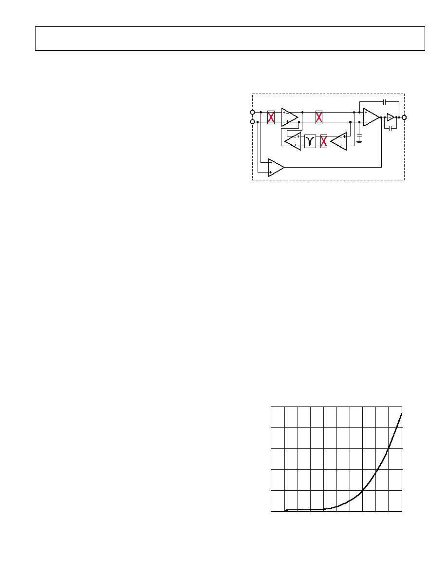
Figure 59 shows the block diagram design of the ADA4051-1/
ADA4051-2 chopper amplifiers employing a local feedback loop
called autocorrection feedback (ACFB). The main signal path
contains an input chopping switch network (CHOP1), a first
transconductance amplifier (Gm1), an output chopping switch
network (CHOP2), a second transconductance amplifier (Gm2),
and a third transconductance amplifier (Gm3). CHOP1 and
CHOP2 operate at 40 kHz of chopping frequency to modulate
the initial offset and 1/f noise from Gm1 up to the chopping
frequency. A fourth transconductance amplifier (Gm4) in the
ACFB senses the modulated ripple at the output of CHOP2,
caused by the initial offset voltage of Gm1. Then, the ripple is
demodulated down to a dc domain through a third chopping
switch network (CHOP3), operating with the same chopping
clock as CHOP1 and CHOP2. Finally, a null transconductance
amplifier (Gm5) tries to null any dc component at the output of
Gm1 that would otherwise appear in the overall output as ripple.
A switched-capacitor notch filter (NF) functions to selectively
suppress the undesired offset-related ripple without disturbing
the desired input signal from the overall input. The desired input
dc signal appears as a dc signal at the output of CHOP2. Then,
the initial offset is modulated up to the chopping frequency by
CHOP3 and filtered out by the NF. Therefore, initial offset does
not create any feedback and does not disturb the desired input
signal. The NF is synchronized with the chopping clock to filter
out the modulated component. In the same manner, the offset
of Gm5 is filtered out by the combination of CHOP3 and the
NF, enabling accurate ripple sensing at the output of CHOP2.
In parallel with the high dc gain path, a feedforward transcon-
ductance amplifier (Gm6) is added to bypass the phase shift
introduced by the ACFB at the chopping frequency. Gm6 is
designed to have the same transconductance as Gm1 to avoid
pole-zero doublets. This design prevents any instability introduced
by the ACFB in the overall feedback loop.
0
805
6-
060
Gm6 (= Gm1)
C2
C1
Gm3
C3
NF
Gm1
Gm2
CHOP1
CHOP2
Gm4
Gm5
CHOP3
OUT
+IN
–IN
Figure 59. ADA4051-1/ADA4051-2 Chopper Amplifiers Block Diagram
The voltage noise density, which is equal to the thermal noise
floor dominated by the Gm1, is essentially flat from dc to the
chopping frequency because CHOP1 and CHOP2 eliminate the
1/f noise generated in Gm1 and the ACFB does not contribute
any additional noise. Although the ACFB suppresses the ripple
related to the chopping, there is a remaining voltage ripple. To
further suppress the remaining ripple down to a desired level, it
is recommended to have a postfilter at the output of the amplifier.
The remaining voltage ripple originates from two sources. The
first type of ripple is due to the residual ripple associated with
the initial offset of the Gm1. It is proportional to the magnitude
of the initial offset and creates a spectrum at the chopping
frequency (fCHOP). When the amplifier is configured as a unity-
gain buffer, this ripple has a typical value of 4.9 μV rms and a
maximum of 34.7 μV rms. The second type of ripple is due to
the intermodulation between the high frequency input signal
and the chopping frequency. This ripple depends on the input
frequency (fIN) and creates a spectrum at frequencies equal to
the difference between the chopping frequency and the input
frequency (fCHOP fIN), as well as at frequencies equal to the
summation of the chopping frequency and the input frequency
(fCHOP + fIN). The magnitude of the ripple for different input
frequencies is shown in Figure 60.
0
100
200
300
400
500
0123456789
10
M
O
DUL
A
T
E
D
O
U
T
P
UT
RI
P
L
E
(
V
rm
s)
INPUT FREQUENCY (kHz)
08
05
6-
0
63
Figure 60. ADA4051-1/ADA4051-2 Modulated Output Ripple vs. Input Frequency
相关PDF资料 |
PDF描述 |
|---|---|
| AD8602ARM-REEL | IC OPAMP GP CMOS 8.4MHZ 8MSOP |
| TSW-106-06-L-S | CONN HEADER 6POS .100" SGL GOLD |
| TSW-107-06-L-S | CONN HEADER 7POS .100" SGL GOLD |
| TSW-108-06-L-S | CONN HEADER 8POS .100" SGL GOLD |
| TSW-109-06-L-S | CONN HEADER 9POS .100" SGL GOLD |
相关代理商/技术参数 |
参数描述 |
|---|---|
| ADA4051-1ARJZ-RL | 功能描述:IC OPAMP R-R CMOS 115KHZ SOT23-5 RoHS:是 类别:集成电路 (IC) >> Linear - Amplifiers - Instrumentation 系列:- 标准包装:160 系列:- 放大器类型:通用 电路数:4 输出类型:满摆幅 转换速率:10 V/µs 增益带宽积:9MHz -3db带宽:- 电流 - 输入偏压:1pA 电压 - 输入偏移:250µV 电流 - 电源:730µA 电流 - 输出 / 通道:28mA 电压 - 电源,单路/双路(±):2.7 V ~ 5.5 V,±1.35 V ~ 2.75 V 工作温度:-40°C ~ 125°C 安装类型:表面贴装 封装/外壳:16-SOIC(0.154",3.90mm 宽) 供应商设备封装:16-SOIC N 包装:管件 |
| ADA4051-2 | 制造商:AD 制造商全称:Analog Devices 功能描述:30 V Zero-Drift, Rail-to-Rail Output Precision Amplifier |
| ADA4051-2_VB | 制造商:AD 制造商全称:Analog Devices 功能描述:Low Cost, Level Shifted Low Side Current Monitor for Negative High Voltage Rails |
| ADA4051-2ACPZ-R2 | 功能描述:IC OPAMP RRIO ZERO DRIFT 8LFCSP RoHS:是 类别:集成电路 (IC) >> Linear - Amplifiers - Instrumentation 系列:- 标准包装:50 系列:- 放大器类型:J-FET 电路数:2 输出类型:- 转换速率:3.5 V/µs 增益带宽积:1MHz -3db带宽:- 电流 - 输入偏压:30pA 电压 - 输入偏移:2000µV 电流 - 电源:200µA 电流 - 输出 / 通道:- 电压 - 电源,单路/双路(±):7 V ~ 36 V,±3.5 V ~ 18 V 工作温度:0°C ~ 70°C 安装类型:通孔 封装/外壳:8-DIP(0.300",7.62mm) 供应商设备封装:8-PDIP 包装:管件 |
| ADA4051-2ACPZ-R7 | 功能描述:IC OPAMP RRIO ZERO DRIFT 8LFCSP RoHS:是 类别:集成电路 (IC) >> Linear - Amplifiers - Instrumentation 系列:- 标准包装:1,000 系列:- 放大器类型:电压反馈 电路数:4 输出类型:满摆幅 转换速率:33 V/µs 增益带宽积:20MHz -3db带宽:30MHz 电流 - 输入偏压:2nA 电压 - 输入偏移:3000µV 电流 - 电源:2.5mA 电流 - 输出 / 通道:30mA 电压 - 电源,单路/双路(±):4.5 V ~ 16.5 V,±2.25 V ~ 8.25 V 工作温度:-40°C ~ 85°C 安装类型:表面贴装 封装/外壳:14-SOIC(0.154",3.90mm 宽) 供应商设备封装:14-SOIC 包装:带卷 (TR) |
发布紧急采购,3分钟左右您将得到回复。