- 您现在的位置:买卖IC网 > PDF目录8586 > ADA4432-1BCPZ-R7 (Analog Devices Inc)IC SD VIDEO FILTER AMP 8LFCSP PDF资料下载
参数资料
| 型号: | ADA4432-1BCPZ-R7 |
| 厂商: | Analog Devices Inc |
| 文件页数: | 27/29页 |
| 文件大小: | 0K |
| 描述: | IC SD VIDEO FILTER AMP 8LFCSP |
| 标准包装: | 1 |
| 应用: | 车载系统 |
| 输出类型: | 单端 |
| 电路数: | 1 |
| -3db带宽: | 10.5MHz |
| 电流 - 电源: | 7.6mA |
| 电流 - 输出 / 通道: | 50mA |
| 电压 - 电源,单路/双路(±): | 2.6 V ~ 3.6 V |
| 安装类型: | 表面贴装 |
| 封装/外壳: | 8-WFDFN 裸露焊盘,CSP |
| 供应商设备封装: | 8-LFCSP-WD(3x3) |
| 包装: | 标准包装 |
| 其它名称: | ADA4432-1BCPZ-R7DKR |
第1页第2页第3页第4页第5页第6页第7页第8页第9页第10页第11页第12页第13页第14页第15页第16页第17页第18页第19页第20页第21页第22页第23页第24页第25页第26页当前第27页第28页第29页
ADA4432-1/ADA4433-1
Data Sheet
Rev. A | Page 6 of 28
ABSOLUTE MAXIMUM RATINGS
Table 3.
Parameter
Rating
Supply Voltage
4 V
Output Common-Mode Voltage
22 V
Input Differential Voltage
+VS
Power Dissipation
Storage Temperature Range
65°C to +125°C
Operating Temperature Range
40°C to +125°C
Lead Temperature (Soldering, 10 sec)
260°C
Junction Temperature
150°C
Stresses above those listed under Absolute Maximum Ratings
may cause permanent damage to the device. This is a stress
rating only; functional operation of the device at these or any
other conditions above those indicated in the operational
section of this specification is not implied. Exposure to absolute
maximum rating conditions for extended periods may affect
device reliability.
THERMAL RESISTANCE
θJA is specified for the device soldered to a high thermal
conductivity 4-layer (2s2p) circuit board, as described in
EIA/JESD 51-7.
Table 4.
Package Type
θJA
θJC
Unit
6-Lead SOT-23
170
Not applicable
°C/W
8-Lead LFCSP
50
5
°C/W
MAXIMUM POWER DISSIPATION
The maximum safe power dissipation in the ADA4432-1 and
ADA4433-1 packages are limited by the associated rise in
junction temperature (TJ) on the die. At approximately 150°C,
which is the glass transition temperature, the plastic changes its
properties. Exceeding a junction temperature of 150°C for an
extended time can result in changes in the silicon devices,
potentially causing failure.
The power dissipated in the package (PD) is the sum of the
quiescent power dissipation and the power dissipated in the
package due to the load drive for all outputs. The quiescent
power is the voltage between the supply pins (VS) times the
quiescent current (IS). The power dissipated due to the load drive
depends on the particular application. For each output, the
power due to load drive is calculated by multiplying the load
current by the associated voltage drop across the device. The
power dissipated due to the loads is equal to the sum of the
power dissipations due to each individual load. RMS voltages
and currents must be used in these calculations.
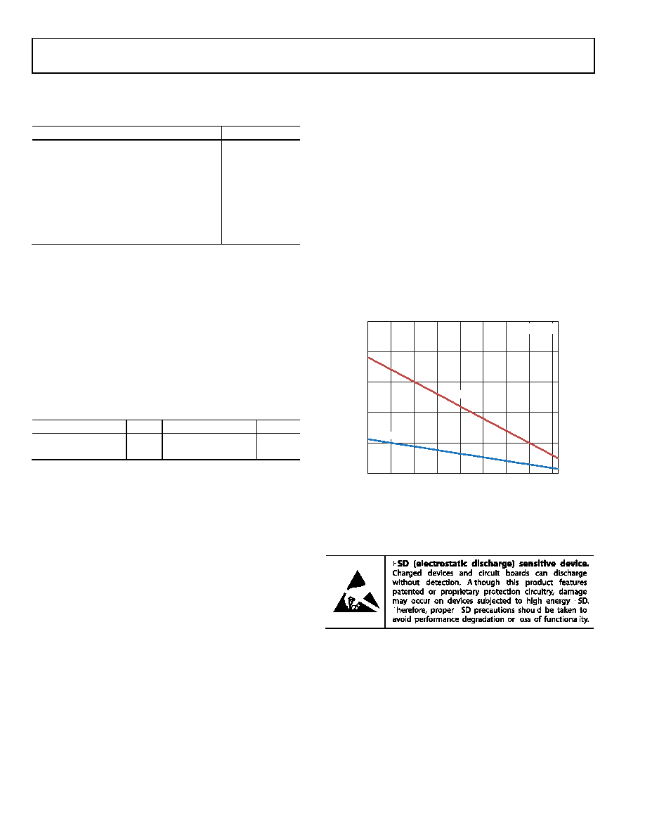
Airflow increases heat dissipation, effectively reducing θJA.
Figure 3 shows the maximum power dissipation in the package
vs. the ambient temperature for the 6-lead SOT-23 (170°C/W)
and the 8-lead LFCSP (50°C/W) on a JEDEC standard 4-layer
board. θJA values are approximate.
Figure 3. Maximum Power Dissipation vs.
Ambient Temperature for a 4-Layer Board
ESD CAUTION
0
1
2
3
4
5
–40
–20
0
20
40
60
80
100
120
MA
XI
MU
M
PO
W
ER
D
ISSI
PA
T
IO
N
(W
)
AMBIENT TEMPERATURE (C)
TJ = 150°C
LFCSP
SOT-23
10597-
003
相关PDF资料 |
PDF描述 |
|---|---|
| AD5541AR | IC DAC 16BIT SRL IN/VOUT 8-SOIC |
| AD767JP | IC DAC 12BIT W/AMP 28-PLCC |
| AD7245JP | IC DAC 12BIT LC2MOS 28-PLCC |
| VE-2W0-IV-F2 | CONVERTER MOD DC/DC 5V 150W |
| AD7245AAP | IC DAC 12BIT W/REF 28-PLCC |
相关代理商/技术参数 |
参数描述 |
|---|---|
| ADA4432-1BRJ-EBZ | 制造商:AD 制造商全称:Analog Devices 功能描述:SD Video Filter Amplifiers |
| ADA4432-1BRJZ-R2 | 制造商:Analog Devices 功能描述:HIGH SPEED VIDEO FILTER AMPLIFIERS - Tape and Reel |
| ADA4432-1BRJZ-R7 | 功能描述:IC SD VIDEO FILTER AMP SOT23-6 RoHS:是 类别:集成电路 (IC) >> 线性 - 放大器 - 视频放大器和频缓冲器 系列:- 标准包装:1,000 系列:- 应用:驱动器 输出类型:差分 电路数:3 -3db带宽:350MHz 转换速率:1000 V/µs 电流 - 电源:14.5mA 电流 - 输出 / 通道:60mA 电压 - 电源,单路/双路(±):5 V ~ 12 V,±2.5 V ~ 6 V 安装类型:表面贴装 封装/外壳:20-VFQFN 裸露焊盘 供应商设备封装:20-QFN 裸露焊盘(4x4) 包装:带卷 (TR) |
| ADA4432-1WBCPZ-R7 | 制造商:AD 制造商全称:Analog Devices 功能描述:SD Video Filter Amplifiers |
| ADA4432-1WBRJZ-R2 | 功能描述:IC SD VIDEO FILTER AMP 6SOT23 制造商:analog devices inc. 系列:- 包装:带卷(TR) 零件状态:过期 应用:车载系统 输出类型:单端 电路数:1 -3db 带宽:10.5MHz 压摆率:- 电流 - 电源:7.6mA 电流 - 输出/通道:50mA 电压 - 电源,单/双(±):2.6 V ~ 3.6 V 安装类型:表面贴装 封装/外壳:SOT-23-6 供应商器件封装:SOT-23 标准包装:250 |
发布紧急采购,3分钟左右您将得到回复。