参数资料
| 型号: | ADA4433-1BCPZ-R7 |
| 厂商: | Analog Devices Inc |
| 文件页数: | 12/16页 |
| 文件大小: | 0K |
| 描述: | IC SD VIDEO FILTER 8LFCSP |
| 标准包装: | 1 |
| 应用: | 重构滤波器 |
| 输出类型: | 差分 |
| 电路数: | 1 |
| -3db带宽: | 9.9MHz |
| 电流 - 电源: | 13.2mA |
| 电流 - 输出 / 通道: | 29mA |
| 电压 - 电源,单路/双路(±): | 2.7 V ~ 3.6 V |
| 安装类型: | 表面贴装 |
| 封装/外壳: | 8-WFDFN 裸露焊盘,CSP |
| 供应商设备封装: | 8-LFCSP-VD(3x3) |
| 包装: | 标准包装 |
| 其它名称: | ADA4433-1BCPZ-R7DKR |
Data Sheet
ADA4433-1
Rev. 0 | Page 5 of 16
ABSOLUTE MAXIMUM RATINGS
Table 2.
Parameter
Rating
Supply Voltage
4 V
Output Common-Mode Voltage
22 V
Input Differential Voltage
+VS
Power Dissipation
See Figure 2
Storage Temperature Range
65°C to +125°C
Operating Temperature Range
40°C to +125°C
Lead Temperature (Soldering, 10 sec)
260°C
Junction Temperature
150°C
Stresses above those listed under Absolute Maximum Ratings
may cause permanent damage to the device. This is a stress
rating only; functional operation of the device at these or any
other conditions above those indicated in the operational
section of this specification is not implied. Exposure to absolute
maximum rating conditions for extended periods may affect
device reliability.
THERMAL RESISTANCE
θJA is specified for the device soldered to a high thermal
conductivity 4-layer (2s2p) circuit board, as described in
EIA/JESD 51-7.
Table 3.
Package Type
θJA
θJC
Unit
8-Lead LFCSP
50
5
°C/W
MAXIMUM POWER DISSIPATION
The maximum safe power dissipation in the ADA4433-1 package
is limited by the associated rise in junction temperature (TJ) on
the die. At approximately 150°C, which is the glass transition
temperature, the plastic changes its properties. Exceeding a
junction temperature of 150°C for an extended time can result
in changes in the silicon devices, potentially causing failure.
The power dissipated in the package (PD) is the sum of the
quiescent power dissipation and the power dissipated in the
package due to the load drive for all outputs. The quiescent
power is the voltage between the supply pins (VS) times the
quiescent current (IS). The power dissipated due to the load
drive depends on the particular application. For each output,
the power due to load drive is calculated by multiplying the load
current by the associated voltage drop across the device. The
power dissipated due to the loads is equal to the sum of the
power dissipations due to each individual load. RMS voltages
and currents must be used in these calculations.
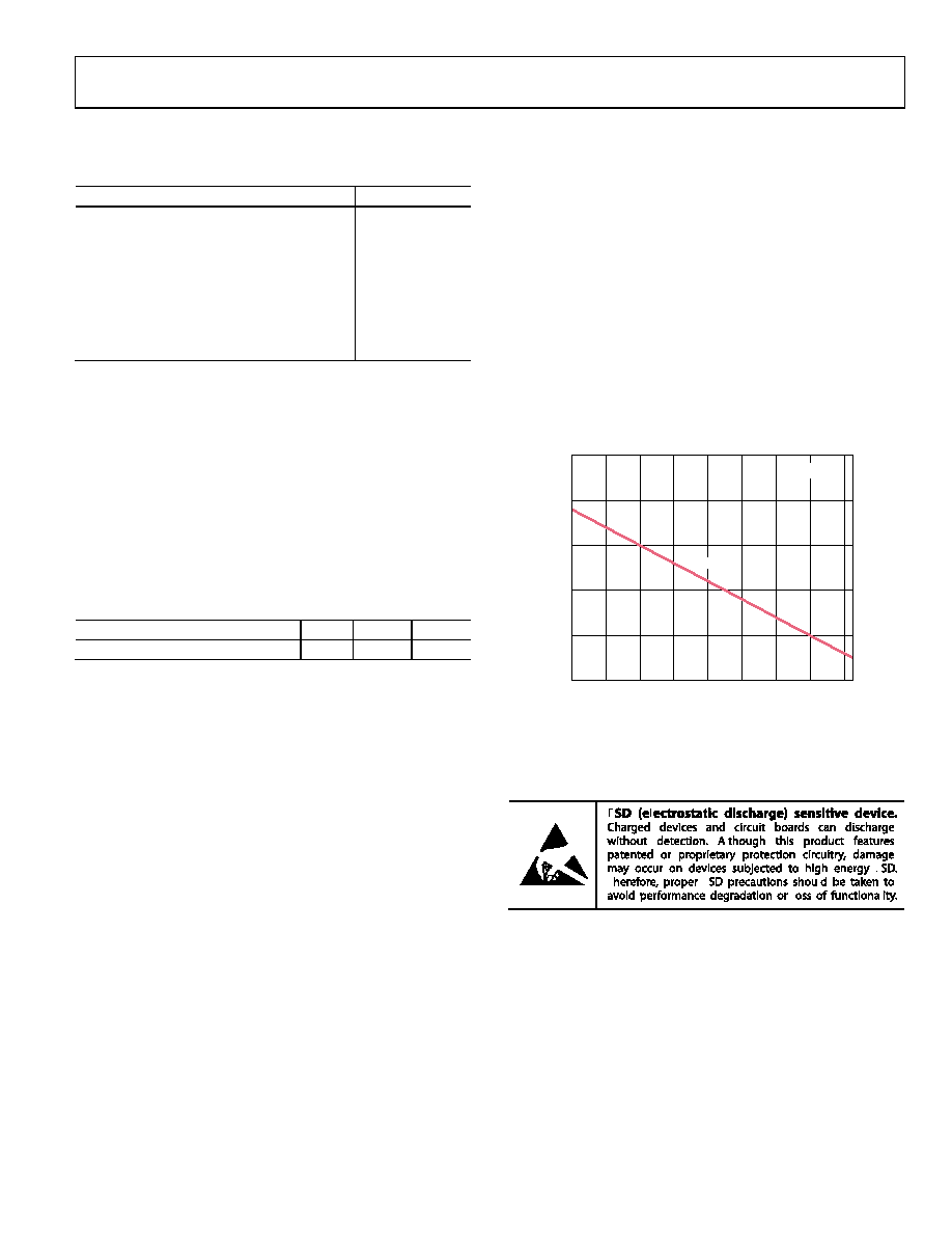
Airflow increases heat dissipation, effectively reducing θJA. Figure 2
shows the maximum power dissipation in the package vs. the
ambient temperature for the 8-lead LFCSP (50°C/W) on a JEDEC
standard 4-layer board. θJA values are approximate.
Figure 2. Maximum Power Dissipation vs.
Ambient Temperature for a 4-Layer Board
ESD CAUTION
0
1
2
3
4
5
–40
–20
0
20
40
60
80
100
120
MA
XI
MU
M
PO
W
ER
D
ISSI
PA
T
IO
N
(W
)
AMBIENT TEMPERATURE (C)
TJ = 150°C
LFCSP
10597-
003
相关PDF资料 |
PDF描述 |
|---|---|
| ADA4853-2YCPZ-R2 | IC OPAMP VIDEO DUAL 16-LFCSP |
| ADA4856-3YCPZ-R2 | IC AMP 3CH RRO VFB G=+2 16LFCSP |
| ADA4859-3ACPZ-RL | IC AMP 3CH CFB G=2 W/CP 16LFCSP |
| ADA4922-1ACPZ-R2 | IC ADC DRIVER 18BIT DIFF 8-LFCSP |
| ADA4937-2YCPZ-RL | IC ADC DRIVER DUAL DIFF 24LFCSP |
相关代理商/技术参数 |
参数描述 |
|---|---|
| ADA4433-1WBCPZ-R7 | 制造商:AD 制造商全称:Analog Devices 功能描述:SD Video Filter Amplifiers |
| ADA4500-2 | 制造商:AD 制造商全称:Analog Devices 功能描述:8.7MHz, 15nV/√Hz, Rail-to-Rail I/O |
| ADA4500-2_12 | 制造商:AD 制造商全称:Analog Devices 功能描述:10 MHz, 14.5 nV/a??Hz, Rail-to-Rail I/O, Zero Input Crossover Distortion Amplifier |
| ADA4500-2_13 | 制造商:AD 制造商全称:Analog Devices 功能描述:10 MHz, 14.5 nV/a??Hz, Rail-to-Rail I/O, Zero Input Crossover Distortion Amplifier |
| ADA4500-2ACPZ-R7 | 制造商:Analog Devices 功能描述:DUAL HIGH PERFORMANCE ZCO OP AMP - Tape and Reel 制造商:Analog Devices 功能描述:IC OPAMP GP 10MHZ RRO 8LFCSP 制造商:Analog Devices 功能描述:DUAL High Performance ZCO Op Amp |
发布紧急采购,3分钟左右您将得到回复。