参数资料
| 型号: | ADA4830-1BCPZ-R7 |
| 厂商: | Analog Devices Inc |
| 文件页数: | 12/16页 |
| 文件大小: | 0K |
| 描述: | IC AMP BATT PROTECT 8LFCSP |
| 标准包装: | 1,500 |
| 放大器类型: | 差分 |
| 电路数: | 1 |
| 转换速率: | 220 V/µs |
| -3db带宽: | 84MHz |
| 电流 - 电源: | 6.8mA |
| 电流 - 输出 / 通道: | 125mA |
| 电压 - 电源,单路/双路(±): | 2.9 V ~ 5.5 V |
| 工作温度: | -40°C ~ 125°C |
| 安装类型: | 表面贴装 |
| 封装/外壳: | 8-WFDFN 裸露焊盘,CSP |
| 供应商设备封装: | 8-LFCSP(3x3) |
| 包装: | 带卷 (TR) |
| 其它名称: | ADA4830-1BCPZ-R7TR |
Data Sheet
ADA4830-1
Rev. 0 | Page 5 of 16
ABSOLUTE MAXIMUM RATINGS
Table 3.
Parameter
Rating
Supply Voltage (+VS pin)
6 V
Input Voltage Positive Direction (INN, INP)
22 V
Input Voltage Negative Direction (INN, INP)
10 V
Reference Voltage (VREF pin)
+V
S + 0.3 V
Power Dissipation
Storage Temperature Range
65°C to +125°C
Operating Temperature Range
40°C to +125°C
Lead Temperature (Soldering, 10 sec)
260°C
Junction Temperature
150°C
THERMAL RESISTANCE
θJA is specified for the device soldered to a high thermal
conductivity, 4-layer (2s2p) circuit board, as described in
EIA/JESD 51-7.
Table 4.
Package Type
θJA
Unit
8-Lead LFCSP
116
°C/W
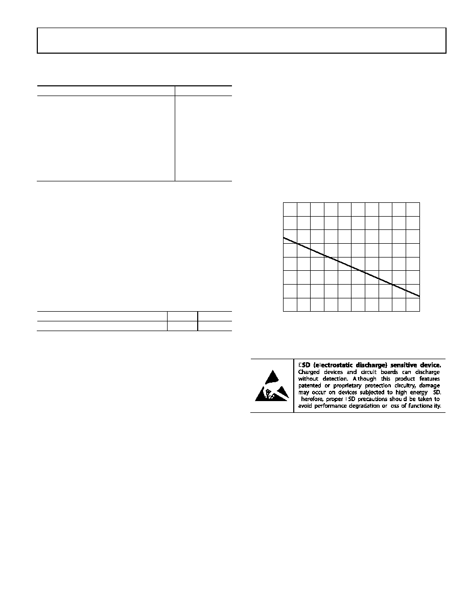
MAXIMUM POWER DISSIPATION
The maximum safe power dissipation in the ADA4830-1
package is limited by the associated rise in junction temperature
(TJ) on the die. At approximately 150°C, which is the glass
transition temperature, the plastic changes its properties.
Exceeding a junction temperature of 150°C for an extended
time can result in changes in the silicon devices, potentially
causing failure.
The power dissipated in the package (PD) is the sum of the
quiescent power dissipation and the power dissipated in the
package due to the load drive for all outputs. The quiescent
power is the voltage between the supply pins (VS) times the
quiescent current (IS). The power dissipated due to load drive
depends on the particular application. The power due to load
drive is calculated by multiplying the load current by the
associated voltage drop across the device. RMS voltages and
currents must be used in these calculations.
Airflow increases heat dissipation, effectively reducing θJA.
Figure 2 shows the maximum power dissipation in the package
vs. the ambient temperature for the 8-lead LFCSP (116°C/W) on
a JEDEC standard 4-layer board. θJA values are approximate.
Figure 2. Maximum Power Dissipation vs.
Ambient Temperature for a 4-Layer Board
ESD CAUTION
Stresses above those listed under Absolute Maximum Ratings
may cause permanent damage to the device. This is a stress
rating only; functional operation of the device at these or any
other conditions above those indicated in the operational
section of this specification is not implied. Exposure to absolute
maximum rating conditions for extended periods may affect
device reliability.
0.2
0.4
0.6
0.8
1.0
1.2
1.4
1.6
1.8
0
10
20
30
40
50
60
70
80
90
100
MA
XI
MU
M
PO
W
ER
D
ISSI
PA
TION
(
W)
AMBIENT TEMPERATURE (°C)
10020-
002
相关PDF资料 |
PDF描述 |
|---|---|
| ADA4830-2BCPZ-R7 | IC AMP BATT PROTECT DUAL 16LFCSP |
| ADA4841-2YRZ-R7 | IC OPAMP VF R-R DUAL LP LN 8SOIC |
| ADA4850-2YCPZ-R2 | IC OPAMP VF R-R DUAL 16LFCSP |
| ADA4851-4YRUZ | IC OPAMP VF R-R QUAD LP 14TSSOP |
| ADA4855-3YCPZ-R7 | IC OPAMP VF R-R TRPL LP 16LFCSP |
相关代理商/技术参数 |
参数描述 |
|---|---|
| ADA4830-1WBCPZ-R7 | 制造商:AD 制造商全称:Analog Devices 功能描述:High Speed Difference Amplifier with Input |
| ADA4830-2 | 制造商:AD 制造商全称:Analog Devices 功能描述:High Speed Difference Amplifier with Input |
| ADA4830-2BCPZ-R2 | 制造商:Analog Devices 功能描述:AMP DIFF DUAL 71MHZ 16LFCSP 制造商:Analog Devices 功能描述:AMP, DIFF, DUAL, 71MHZ, 16LFCSP |
| ADA4830-2BCPZ-R7 | 功能描述:IC AMP BATT PROTECT DUAL 16LFCSP RoHS:是 类别:集成电路 (IC) >> Linear - Amplifiers - Instrumentation 系列:- 产品培训模块:Differential Circuit Design Techniques for Communication Applications 标准包装:1 系列:- 放大器类型:RF/IF 差分 电路数:1 输出类型:差分 转换速率:9800 V/µs 增益带宽积:- -3db带宽:2.9GHz 电流 - 输入偏压:3µA 电压 - 输入偏移:- 电流 - 电源:40mA 电流 - 输出 / 通道:- 电压 - 电源,单路/双路(±):3 V ~ 3.6 V 工作温度:-40°C ~ 85°C 安装类型:表面贴装 封装/外壳:16-VQFN 裸露焊盘,CSP 供应商设备封装:16-LFCSP-VQ 包装:剪切带 (CT) 产品目录页面:551 (CN2011-ZH PDF) 其它名称:ADL5561ACPZ-R7CT |
| ADA4830-2WBCPZ-R7 | 制造商:AD 制造商全称:Analog Devices 功能描述:High Speed Difference Amplifier with Input |
发布紧急采购,3分钟左右您将得到回复。