参数资料
| 型号: | ADA4830-1BCPZ-R7 |
| 厂商: | Analog Devices Inc |
| 文件页数: | 3/16页 |
| 文件大小: | 0K |
| 描述: | IC AMP BATT PROTECT 8LFCSP |
| 标准包装: | 1,500 |
| 放大器类型: | 差分 |
| 电路数: | 1 |
| 转换速率: | 220 V/µs |
| -3db带宽: | 84MHz |
| 电流 - 电源: | 6.8mA |
| 电流 - 输出 / 通道: | 125mA |
| 电压 - 电源,单路/双路(±): | 2.9 V ~ 5.5 V |
| 工作温度: | -40°C ~ 125°C |
| 安装类型: | 表面贴装 |
| 封装/外壳: | 8-WFDFN 裸露焊盘,CSP |
| 供应商设备封装: | 8-LFCSP(3x3) |
| 包装: | 带卷 (TR) |
| 其它名称: | ADA4830-1BCPZ-R7TR |
Data Sheet
ADA4830-1
Rev. 0 | Page 11 of 16
APPLICATIONS INFORMATION
METHODS OF TRANSMISSION
Pseudo Differential Mode (Unbalanced Source
Termination)
The ADA4830-1 can be operated in a pseudo differential
configuration with an unbalanced input signal. This allows
the receiver to be driven by any single-ended source. Pseudo
differential mode uses a single conductor to carry an unbalanced
signal, and connects the negative input terminal to the ground
reference of the source.
Use the positive wire or coaxial center conductor to connect the
source output to the positive input (INP) of the ADA4830-1.
Next, connect the negative wire or coaxial shield from the
negative input (INN) back to a ground reference on the source
printed circuit board (PCB). The input termination should
match the source impedance and be referenced to the remote
ground. An example of this configuration is shown in Figure 21.
Figure 21. Pseudo Differential Mode
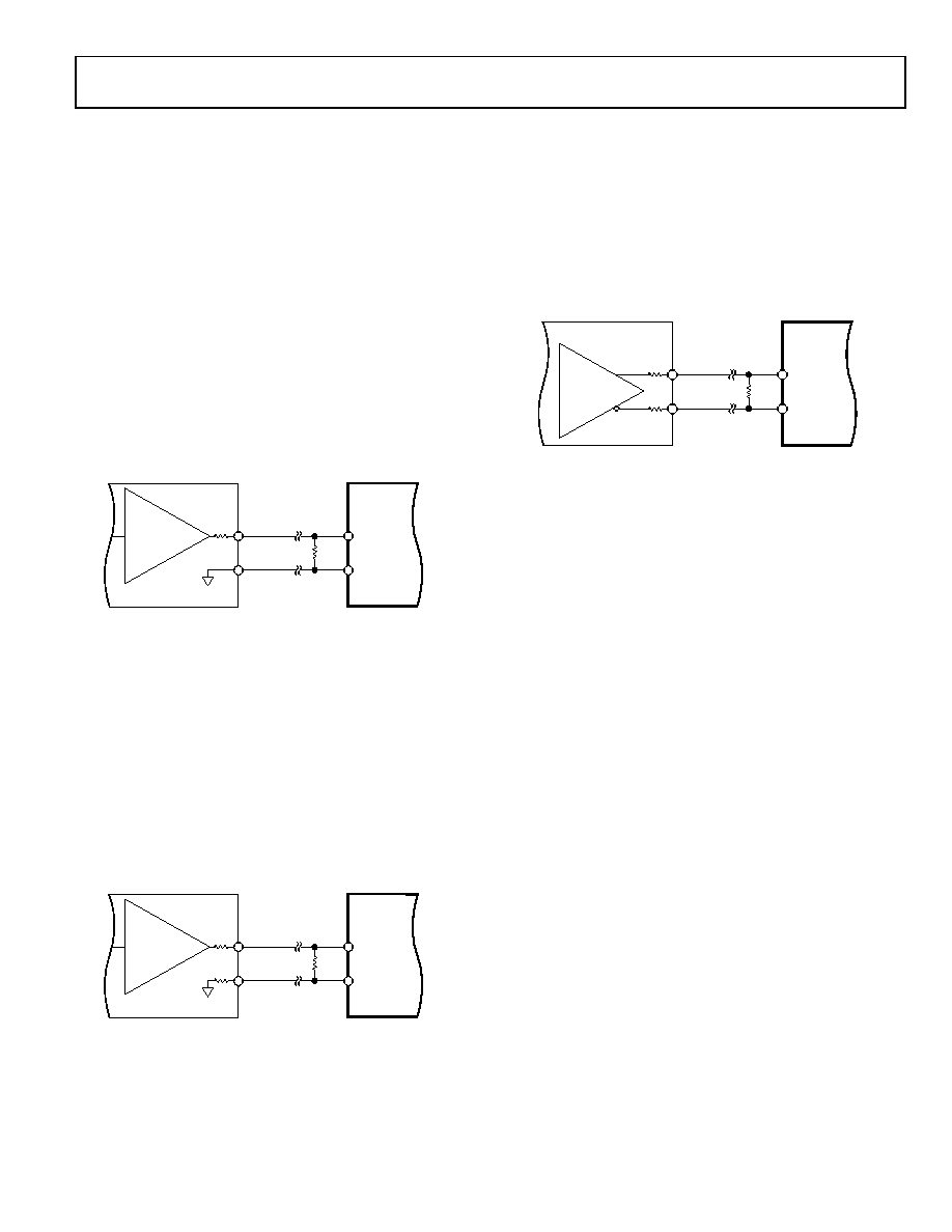
Pseudo Differential Mode (Balanced Source Impedance)
Pseudo differential signaling is typically implemented using
unbalanced source termination as shown in Figure 21. With this
arrangement, however, common-mode signals on the positive
and negative inputs receive different attenuation due to unbalanced
termination at the source. This effectively converts some of the
common-mode signal into differential mode signal, degrading
the overall common-mode rejection of the system. System
common-mode rejection can be improved by balancing the
output impedance of the driver as shown in Figure 22. Splitting
the source termination resistance evenly between the hot and
cold conductors results in matched attenuation of the common-
mode signals, ensuring maximum rejection.
Figure 22. Pseudo Differential Mode with Balanced Source Impedance
Fully Differential Mode
The differential inputs of the ADA4830-1 allow full balanced
transmission using any differential source. In this configuration,
the differential input termination is equal to twice the source
impedance of each output. For example, a source with 37.5
back termination resistors in each leg should be terminated
with a differential resistance of 75 . An illustration of this
arrangement is shown in Figure 23.
Figure 23. Fully Differential Mode
VOLTAGE REFERENCE (VREF PIN)
An internal reference level determines the output voltage when
the differential input voltage is zero. This is set by a resistor
divider connected between the supply rails. Built with a matched
pair of 40 k resistors, the divider sets this voltage to +VS/2.
The voltage reference pin (VREF) normally floats at its default
value of +VS/2. However, it can be used to vary the output
reference level from this default value. A voltage applied to
VREF appears at the output with unity gain, within the
bandwidth limit of the internal reference buffer.
Any noise on the +VS supply rail appears at the output with only
6 dB of attenuation (the divide-by-two provided by the reference
divider). Even when this pin is floating, it is recommended that
an external capacitor be connected from the reference node to
ground to provide further attenuation of noise on the power supply
line. A 4.7 F capacitor combined with the internal 40 k resistor
sets the low-pass corner at under 1 Hz and results in better than
40 dB of supply noise attenuation at 100 Hz.
INPUT COMMON-MODE RANGE
In a standard four resistor difference amplifier with 0.5 V/V
gain, the input common-mode (CM) range is three times the
CM range of the core amplifier. In the ADA4830-1, however,
the input CM has been extended to more than 17 V (with a 5 V
supply). The input CM range can be approximated by using the
following formulas:
Maximum CM voltage
5(+VS 1.25) 4VREF ≈ VINCM(MAX) ≤ 9.5 V
Minimum CM voltage
10 V ≤ VINCM(MIN) ≈ (1 + 4VREF)
INN
INP
ADA4830-1
75
+
75
POSITIVE WIRE
NEGATIVE WIRE
DRIVER PCB
SINGLE ENDED
AMPLIFIER
10020-
034
INN
INP
ADA4830-1
75
+
37.5
37.5
POSITIVE WIRE
NEGATIVE WIRE
DRIVER PCB
10020-
035
SINGLE ENDED
AMPLIFIER
INN
INP
ADA4830-1
75
+
37.5
37.5
POSITIVE WIRE
NEGATIVE WIRE
DRIVER PCB
10020-
036
DIFFERENTIAL
AMPLIFIER
相关PDF资料 |
PDF描述 |
|---|---|
| ADA4830-2BCPZ-R7 | IC AMP BATT PROTECT DUAL 16LFCSP |
| ADA4841-2YRZ-R7 | IC OPAMP VF R-R DUAL LP LN 8SOIC |
| ADA4850-2YCPZ-R2 | IC OPAMP VF R-R DUAL 16LFCSP |
| ADA4851-4YRUZ | IC OPAMP VF R-R QUAD LP 14TSSOP |
| ADA4855-3YCPZ-R7 | IC OPAMP VF R-R TRPL LP 16LFCSP |
相关代理商/技术参数 |
参数描述 |
|---|---|
| ADA4830-1WBCPZ-R7 | 制造商:AD 制造商全称:Analog Devices 功能描述:High Speed Difference Amplifier with Input |
| ADA4830-2 | 制造商:AD 制造商全称:Analog Devices 功能描述:High Speed Difference Amplifier with Input |
| ADA4830-2BCPZ-R2 | 制造商:Analog Devices 功能描述:AMP DIFF DUAL 71MHZ 16LFCSP 制造商:Analog Devices 功能描述:AMP, DIFF, DUAL, 71MHZ, 16LFCSP |
| ADA4830-2BCPZ-R7 | 功能描述:IC AMP BATT PROTECT DUAL 16LFCSP RoHS:是 类别:集成电路 (IC) >> Linear - Amplifiers - Instrumentation 系列:- 产品培训模块:Differential Circuit Design Techniques for Communication Applications 标准包装:1 系列:- 放大器类型:RF/IF 差分 电路数:1 输出类型:差分 转换速率:9800 V/µs 增益带宽积:- -3db带宽:2.9GHz 电流 - 输入偏压:3µA 电压 - 输入偏移:- 电流 - 电源:40mA 电流 - 输出 / 通道:- 电压 - 电源,单路/双路(±):3 V ~ 3.6 V 工作温度:-40°C ~ 85°C 安装类型:表面贴装 封装/外壳:16-VQFN 裸露焊盘,CSP 供应商设备封装:16-LFCSP-VQ 包装:剪切带 (CT) 产品目录页面:551 (CN2011-ZH PDF) 其它名称:ADL5561ACPZ-R7CT |
| ADA4830-2WBCPZ-R7 | 制造商:AD 制造商全称:Analog Devices 功能描述:High Speed Difference Amplifier with Input |
发布紧急采购,3分钟左右您将得到回复。