- 您现在的位置:买卖IC网 > PDF目录16929 > ADA4857-2YCP-EBZ (Analog Devices Inc)BOARD EVAL FOR ADA4857-2YCP PDF资料下载
参数资料
| 型号: | ADA4857-2YCP-EBZ |
| 厂商: | Analog Devices Inc |
| 文件页数: | 17/20页 |
| 文件大小: | 0K |
| 描述: | BOARD EVAL FOR ADA4857-2YCP |
| 标准包装: | 1 |
| 每 IC 通道数: | 2 - 双 |
| 放大器类型: | 电压反馈 |
| 板类型: | 裸(未填充) |
| 已供物品: | 板 |
| 已用 IC / 零件: | 16-LFCSP 封装 |
ADA4857-1/ADA4857-2
Data Sheet
Rev. C | Page 6 of 20
ABSOLUTE MAXIMUM RATINGS
Table 3.
Parameter
Rating
Supply Voltage
11 V
Power Dissipation
Common-Mode Input Voltage
VS + 0.7 V to +VS 0.7 V
Differential Input Voltage
±VS
Exposed Paddle Voltage
VS
Storage Temperature Range
65°C to +125°C
Operating Temperature Range
40°C to +125°C
Lead Temperature (Soldering, 10 sec)
300°C
Junction Temperature
150°C
Stresses above those listed under Absolute Maximum Ratings
may cause permanent damage to the device. This is a stress
rating only; functional operation of the device at these or any
other conditions above those indicated in the operational
section of this specification is not implied. Exposure to absolute
maximum rating conditions for extended periods may affect
device reliability.
THERMAL RESISTANCE
θJA is specified for the worst-case conditions, that is, θJA is specified
for device soldered in circuit board for surface-mount packages.
Table 4.
Package Type
θJA
θJC
Unit
8-Lead SOIC
115
15
°C/W
8-Lead LFCSP
94.5
34.8
°C/W
16-Lead LFCSP
68.2
19
°C/W
MAXIMUM POWER DISSIPATION
The maximum safe power dissipation for the ADA4857 is
limited by the associated rise in junction temperature (TJ) on
the die. At approximately 150°C, which is the glass transition
temperature, the properties of the plastic change. Even temporarily
exceeding this temperature limit may change the stresses that
the package exerts on the die, permanently shifting the parametric
performance of the ADA4857. Exceeding a junction temperature of
175°C for an extended period can result in changes in silicon
devices, potentially causing degradation or loss of functionality.
The power dissipated in the package (PD) is the sum of the
quiescent power dissipation and the power dissipated in the
die due to the ADA4857 drive at the output. The quiescent
power is the voltage between the supply pins (VS) times the
quiescent current (IS).
PD = Quiescent Power + (Total Drive Power Load Power)
(
)
L
OUT
L
OUT
S
D
R
V
R
V
I
V
P
2
–
2
×
+
×
=
RMS output voltages should be considered. If RL is referenced
to VS, as in single-supply operation, the total drive power is
VS × IOUT. If the rms signal levels are indeterminate, consider the
worst case, when VOUT = VS/4 for RL to midsupply.
(
) (
)
L
S
D
R
V
I
V
P
2
4
/
+
×
=
In single-supply operation with RL referenced to VS, the worst
case is VOUT = VS/2.
Airflow increases heat dissipation, effectively reducing θJA.
In addition, more metal directly in contact with the package
leads and exposed paddle from metal traces, through holes,
ground, and power planes reduces θJA.
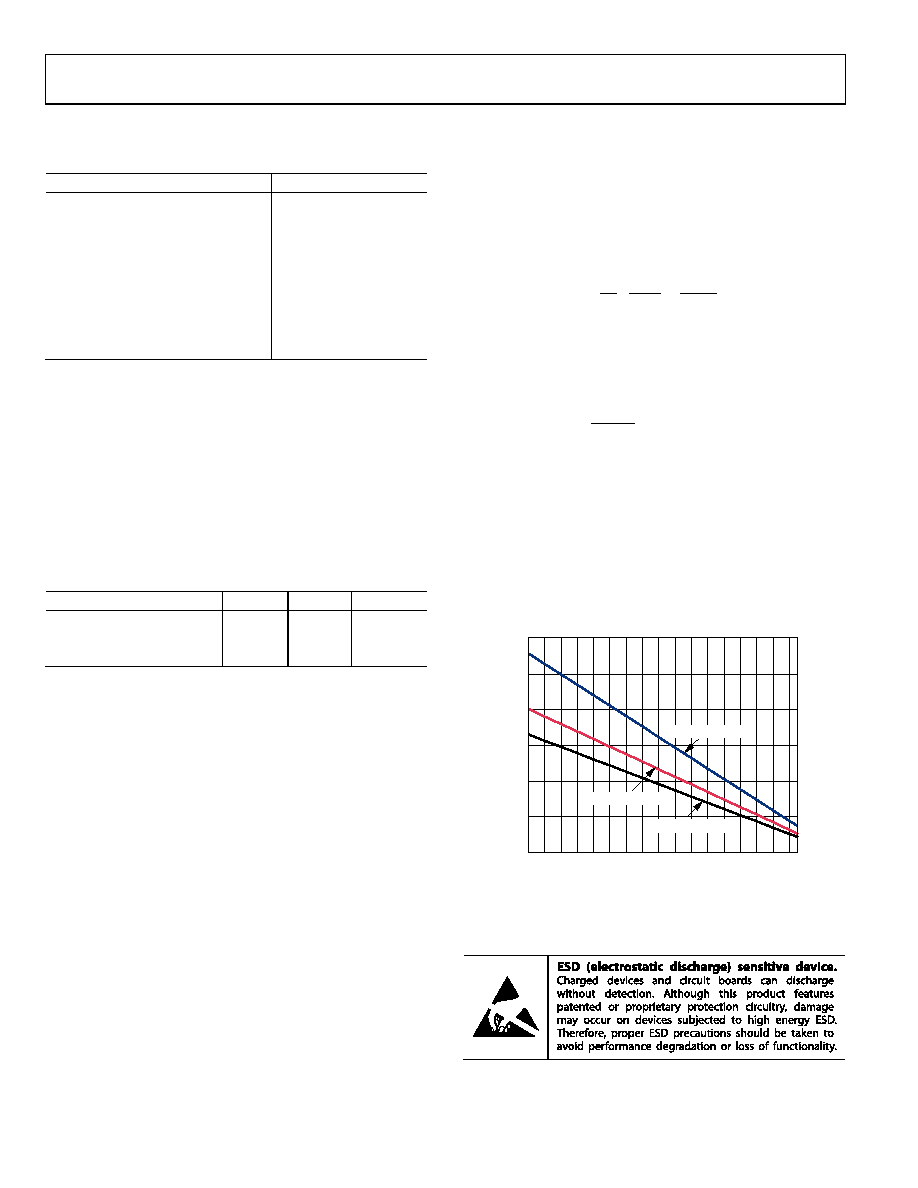
Figure 4 shows the maximum power dissipation in the package
vs. the ambient temperature for the SOIC and LFCSP packages
on a JEDEC standard 4-layer board. θJA values are approximations.
0
0.5
1.0
1.5
2.0
2.5
3.0
–40 –30 –20 –10 0
10 20 30 40 50 60 70 80 90 100 110 120
07040-
004
AMBIENT TEMPERATURE (°C)
MA
XI
MU
M
PO
W
ER
D
ISSI
PA
T
IO
N
(W
)
ADA4857-1 (SOIC)
ADA4857-1 (LFCSP)
ADA4857-2 (LFCSP)
Figure 4. Maximum Power Dissipation vs. Temperature for a 4-Layer Board
ESD CAUTION
相关PDF资料 |
PDF描述 |
|---|---|
| ADA4891-1ARJ-EBZ | BOARD EVAL FOR ADA4891-1ARJ |
| GCC35DCMD | CONN EDGECARD 70POS .100" WW |
| GBC36DCMD | CONN EDGECARD 72POS .100" WW |
| PM105SB-220M-RC | INDUCTOR POWER 22UH SHIELD SMD |
| 0982660901 | CBL 21POS 0.5MM JMPR TYPE A 2" |
相关代理商/技术参数 |
参数描述 |
|---|---|
| ADA4857-2YCPZ-R2 | 制造商:Analog Devices 功能描述:OP Amp Dual Volt Fdbk 制造商:Analog Devices 功能描述:OP AMP DUAL VOLT FDBK 5.25V/10.5V 16LFCSP EP - Tape and Reel 制造商:Analog Devices 功能描述:OP Amp Dual Volt Fdbk }5.25V/10.5V 16-Pin LFCSP EP |
| ADA4857-2YCPZ-R7 | 功能描述:IC OPAMP VF DUAL ULDIST 16LFCSP RoHS:是 类别:集成电路 (IC) >> Linear - Amplifiers - Instrumentation 系列:- 产品培训模块:Differential Circuit Design Techniques for Communication Applications 标准包装:1 系列:- 放大器类型:RF/IF 差分 电路数:1 输出类型:差分 转换速率:9800 V/µs 增益带宽积:- -3db带宽:2.9GHz 电流 - 输入偏压:3µA 电压 - 输入偏移:- 电流 - 电源:40mA 电流 - 输出 / 通道:- 电压 - 电源,单路/双路(±):3 V ~ 3.6 V 工作温度:-40°C ~ 85°C 安装类型:表面贴装 封装/外壳:16-VQFN 裸露焊盘,CSP 供应商设备封装:16-LFCSP-VQ 包装:剪切带 (CT) 产品目录页面:551 (CN2011-ZH PDF) 其它名称:ADL5561ACPZ-R7CT |
| ADA4857-2YCPZ-RL | 功能描述:IC OPAMP VF DUAL ULDIST 16LFCSP RoHS:是 类别:集成电路 (IC) >> Linear - Amplifiers - Instrumentation 系列:- 标准包装:100 系列:- 放大器类型:通用 电路数:1 输出类型:- 转换速率:0.2 V/µs 增益带宽积:- -3db带宽:- 电流 - 输入偏压:100pA 电压 - 输入偏移:30µV 电流 - 电源:380µA 电流 - 输出 / 通道:- 电压 - 电源,单路/双路(±):±2 V ~ 18 V 工作温度:0°C ~ 70°C 安装类型:表面贴装 封装/外壳:8-SOIC(0.154",3.90mm 宽) 供应商设备封装:8-SO 包装:管件 |
| ADA4858-3 | 制造商:AD 制造商全称:Analog Devices 功能描述:Single-Supply, High Speed, Triple Op Amp with Charge Pump |
| ADA4858-3ACP-EBZ | 功能描述:BOARD EVAL FOR ADA4858-3ACP RoHS:是 类别:编程器,开发系统 >> 评估板 - 运算放大器 系列:- 产品培训模块:Lead (SnPb) Finish for COTS Obsolescence Mitigation Program 标准包装:1 系列:- |
发布紧急采购,3分钟左右您将得到回复。