- 您现在的位置:买卖IC网 > PDF目录5265 > ADA4899-1YRDZ-RL (Analog Devices Inc)IC OPAMP VF ULN ULDIST 8SOIC PDF资料下载
参数资料
| 型号: | ADA4899-1YRDZ-RL |
| 厂商: | Analog Devices Inc |
| 文件页数: | 18/21页 |
| 文件大小: | 0K |
| 描述: | IC OPAMP VF ULN ULDIST 8SOIC |
| 产品培训模块: | Practical Guide High Speed PCB Layout |
| 设计资源: | High Speed, Precision, Differential AC-Coupled Drive Circuit for AD7625 (CN0080) |
| 标准包装: | 2,500 |
| 放大器类型: | 电压反馈 |
| 电路数: | 1 |
| 转换速率: | 310 V/µs |
| -3db带宽: | 600MHz |
| 电流 - 输入偏压: | 6µA |
| 电压 - 输入偏移: | 35µV |
| 电流 - 电源: | 14.7mA |
| 电流 - 输出 / 通道: | 200mA |
| 电压 - 电源,单路/双路(±): | 4.5 V ~ 12 V,±2.25 V ~ 6 V |
| 工作温度: | -40°C ~ 125°C |
| 安装类型: | 表面贴装 |
| 封装/外壳: | 8-SOIC(0.154",3.90mm Width)裸露焊盘 |
| 供应商设备封装: | 8-SOIC-EP |
| 包装: | 带卷 (TR) |
ADA4899-1
Rev. B | Page 5 of 20
ABSOLUTE MAXIMUM RATINGS
Table 3.
Parameter
Rating
Supply Voltage
12.6 V
Power Dissipation
See Figure 4
Differential Input Voltage
±1.2 V
Differential Input Current
±10 mA
Storage Temperature Range
–65°C to +150°C
Operating Temperature Range
–40°C to +125°C
Lead Temperature (Soldering 10 sec)
300°C
Junction Temperature
150°C
Stresses above those listed under Absolute Maximum Ratings
may cause permanent damage to the device. This is a stress
rating only; functional operation of the device at these or any
other conditions above those indicated in the operational
section of this specification is not implied. Exposure to absolute
maximum rating conditions for extended periods may affect
device reliability.
MAXIMUM POWER DISSIPATION
The maximum safe power dissipation in the ADA4899-1
package is limited by the associated rise in junction temperature
(TJ) on the die. The plastic encapsulating the die locally reaches
the junction temperature. At approximately 150°C, which is the
glass transition temperature, the plastic changes its properties.
Even temporarily exceeding this temperature limit may change
the stresses that the package exerts on the die, permanently
shifting the parametric performance of the ADA4899-1.
Exceeding a junction temperature of 150°C for an extended
period can result in changes in silicon devices, potentially
causing failure.
The still-air thermal properties of the package and PCB (θJA),
the ambient temperature (TA), and the total power dissipated in
the package (PD) determine the junction temperature of the die.
The junction temperature is calculated as
TJ = TA + (PD × θJA)
The power dissipated in the package (PD) is the sum of the
quiescent power dissipation and the power dissipated in the
package due to the load drive for all outputs. The quiescent
power is the voltage between the supply pins (VS) times the
quiescent current (IS). Assuming the load (RL) is referenced to
midsupply, the total drive power is VS/2 × IOUT, some of which is
dissipated in the package and some in the load (VOUT × IOUT).
The difference between the total drive power and the load
power is the drive power dissipated in the package.
PD = Quiescent Power + (Total Drive Power – Load Power)
()
L
OUT
L
OUT
S
D
R
V
R
V
I
V
P
2
–
2
×
+
×
=
RMS output voltages should be considered. If RL is referenced to
VS–, as in single-supply operation, the total drive power is VS ×
IOUT. If the rms signal levels are indeterminate, consider the
worst case, when VOUT = VS/4 for RL to midsupply
() (
)
L
S
D
R
/
V
I
V
P
2
4
+
×
=
In single-supply operation with RL referenced to VS–, worst case
is VOUT = VS/2.
Airflow increases heat dissipation, effectively reducing θJA. In
addition, more metal directly in contact with the package leads
from metal traces, through holes, ground, and power planes
reduces the θJA. Soldering the exposed paddle to the ground
plane significantly reduces the overall thermal resistance of the
package.
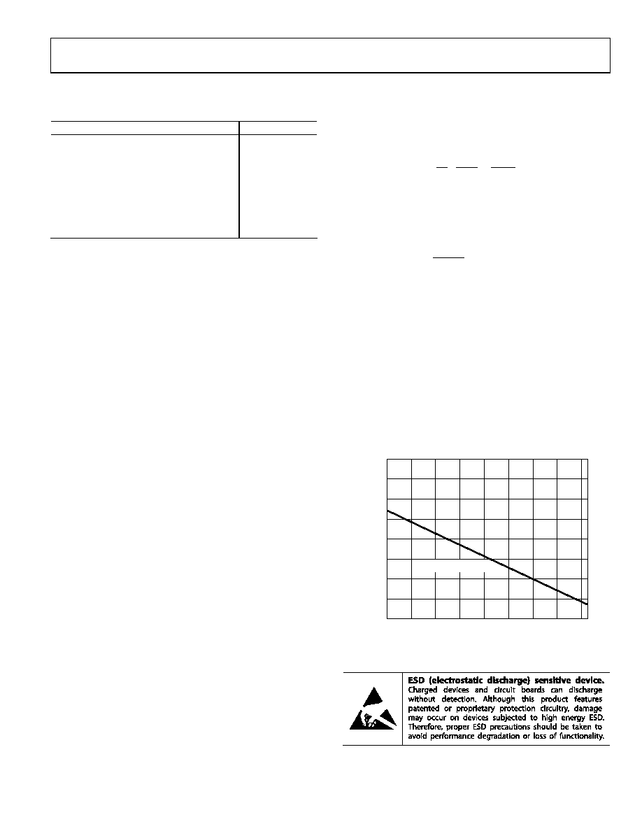
Figure 4 shows the maximum safe power dissipation in the
package vs. the ambient temperature for the exposed paddle
(EPAD) 8-lead SOIC (70°C/W) and 8-lead LFCSP (70°C/W)
packages on a JEDEC standard 4-layer board. θJA values are
approximations.
05
720-
00
3
AMBIENT TEMPERATURE (°C)
120
–40
–20
0
204060
80
100
MA
XI
M
U
M
PO
W
E
R
D
ISS
IP
A
T
IO
N
(
W
)
0.0
4.0
3.5
3.0
2.5
2.0
1.5
1.0
0.5
LFCSP AND SOIC
Figure 4. Maximum Power Dissipation vs. Ambient Temperature
ESD CAUTION
相关PDF资料 |
PDF描述 |
|---|---|
| EL5410CR-T13 | IC AMP QUAD R-R I/O 30MHZ 14-TSS |
| TA45-ABDRF200C0 | CIRCUIT BRKR THERMAL 20A 2POLE |
| AD8028ARMZ-REEL | IC OPAMP R-R DUAL LDIST 10MSOP |
| LT6002CDHC#PBF | IC OP AMP R-R 1.8V QUAD 16-DFN |
| 150218-6002-RB | CONN 18POS 2MM SOCKET VERT PC MT |
相关代理商/技术参数 |
参数描述 |
|---|---|
| ADA4922-1 | 制造商:AD 制造商全称:Analog Devices 功能描述:14-Bit, 1 MSPS, Differential, Programmable Input PulSAR ADC |
| ADA4922-1ACP-EBZ | 功能描述:BOARD EVAL FOR ADA4922-1ACP RoHS:是 类别:编程器,开发系统 >> 评估板 - 运算放大器 系列:- 产品培训模块:Lead (SnPb) Finish for COTS Obsolescence Mitigation Program 标准包装:1 系列:- |
| ADA4922-1ACPZ-R2 | 功能描述:IC ADC DRIVER 18BIT DIFF 8-LFCSP RoHS:是 类别:集成电路 (IC) >> 线性 - 放大器 - 专用 系列:- 产品培训模块:Lead (SnPb) Finish for COTS Obsolescence Mitigation Program 标准包装:60 系列:- 类型:可变增益放大器 应用:CATV 安装类型:表面贴装 封装/外壳:20-WQFN 裸露焊盘 供应商设备封装:20-TQFN-EP(5x5) 包装:托盘 |
| ADA4922-1ACPZ-R7 | 制造商:Analog Devices 功能描述:SP AMP DIFF LINE DRVR AMP SGL R-R O/P 26V 8LFCSP EP - Bulk |
| ADA4922-1ACPZ-RL | 功能描述:IC ADC DRIVER 18BIT DIFF 8-LFCSP RoHS:是 类别:集成电路 (IC) >> 线性 - 放大器 - 专用 系列:- 产品培训模块:Lead (SnPb) Finish for COTS Obsolescence Mitigation Program 标准包装:60 系列:- 类型:可变增益放大器 应用:CATV 安装类型:表面贴装 封装/外壳:20-WQFN 裸露焊盘 供应商设备封装:20-TQFN-EP(5x5) 包装:托盘 |
发布紧急采购,3分钟左右您将得到回复。