- 您现在的位置:买卖IC网 > PDF目录5265 > ADA4899-1YRDZ-RL (Analog Devices Inc)IC OPAMP VF ULN ULDIST 8SOIC PDF资料下载
参数资料
| 型号: | ADA4899-1YRDZ-RL |
| 厂商: | Analog Devices Inc |
| 文件页数: | 9/21页 |
| 文件大小: | 0K |
| 描述: | IC OPAMP VF ULN ULDIST 8SOIC |
| 产品培训模块: | Practical Guide High Speed PCB Layout |
| 设计资源: | High Speed, Precision, Differential AC-Coupled Drive Circuit for AD7625 (CN0080) |
| 标准包装: | 2,500 |
| 放大器类型: | 电压反馈 |
| 电路数: | 1 |
| 转换速率: | 310 V/µs |
| -3db带宽: | 600MHz |
| 电流 - 输入偏压: | 6µA |
| 电压 - 输入偏移: | 35µV |
| 电流 - 电源: | 14.7mA |
| 电流 - 输出 / 通道: | 200mA |
| 电压 - 电源,单路/双路(±): | 4.5 V ~ 12 V,±2.25 V ~ 6 V |
| 工作温度: | -40°C ~ 125°C |
| 安装类型: | 表面贴装 |
| 封装/外壳: | 8-SOIC(0.154",3.90mm Width)裸露焊盘 |
| 供应商设备封装: | 8-SOIC-EP |
| 包装: | 带卷 (TR) |
ADA4899-1
Rev. B | Page 16 of 20
DISABLE PIN OPERATION
The ADA4899-1 DISABLE pin performs three functions:
enable, disable, and reduction of the input bias current. When
the DISABLE pin is brought to within 0.7 V of the positive
supply, the input bias current circuit is enabled, which reduces
the input bias current by a factor of 100. In this state, the input
current noise doubles from 2.6 pA/√Hz to 5.2 pA/√Hz. Table 7
outlines the DISABLE pin operation.
Table 7. DISABLE Pin Truth Table
Supply Voltage
±5 V
+5 V
Disable
5 V to +2.4 V
0 V to 2.4 V
Enable
Open
Low Input Bias Current
4.3 V to 5 V
ADA4899-1 MUX
With a true output disable, the ADA4899-1 can be used in
multiplexer applications. The outputs of two ADA4899-1s are
wired together to form a 2:1 mux. Figure 51 shows the 2:1 mux
schematic.
05720
-0
64
1MHz
0V TO 5V
+5V
–5V
+5V
–5V
0.1F
ADA4899-1
2V p-p
15MHz
+5V
–5V
0.1F
ADA4899-1
0.1F
2.2F
0.1F
2.2F
+
2k
1k
50
1.02k
50
VREF = 2.50V
2k
1V p-p
15MHz
DISABLE
AD8137
DISABLE
50
RT
50
VOUT
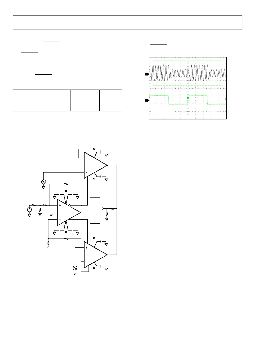
Figure 51. ADA4899-1 2:1 Mux Schematic
An AD8137 differential amplifier is used as a level translator
that converts the TTL input to a complementary ±3 V output to
drive the DISABLE pins of the ADA4899-1s. The transient
response for the 2:1 mux is shown in Figure 52.
05
72
0-
06
5
2
1
CH1 = 500mV/DIV
CH2 = 5V/DIV
200ns/DIV
Figure 52. ADA4899-1 2:1 Mux Transient Response
CIRCUIT CONSIDERATIONS
Careful and deliberate attention to detail when laying out the
ADA4899-1 board yields optimal performance. Power supply
bypassing, parasitic capacitance, and component selection all
contribute to the overall performance of the amplifier.
PCB Layout
Because the ADA4899-1 can operate up to 600 MHz, it is
essential that RF board layout techniques be employed. All
ground and power planes under the pins of the ADA4899-1
should be cleared of copper to prevent the formation of parasitic
capacitance between the input pins to ground and the output
pins to ground. A single mounting pad on a SOIC footprint can
add as much as 0.2 pF of capacitance to ground if the ground
plane is not cleared from under the mounting pads. The low
distortion pinout of the ADA4899-1 reduces the distance
between the output and the inverting input of the amplifier.
This helps minimize the parasitic inductance and capacitance
of the feedback path, which reduces ringing and second harmonic
distortion.
Power Supply Bypassing
Power supply bypassing for the ADA4899-1 has been optimized
for frequency response and distortion performance. Figure 40
shows the recommended values and location of the bypass
capacitors. Power supply bypassing is critical for stability,
frequency response, distortion, and PSR performance. The
0.1 μF capacitors shown in Figure 40 should be as close to the
supply pins of the ADA4899-1 as possible. The electrolytic
capacitors should be directly adjacent to the 0.1 μF capacitors.
The capacitor between the two supplies helps improve PSR and
distortion performance. In some cases, additional paralleled
capacitors can help improve frequency and transient response.
相关PDF资料 |
PDF描述 |
|---|---|
| EL5410CR-T13 | IC AMP QUAD R-R I/O 30MHZ 14-TSS |
| TA45-ABDRF200C0 | CIRCUIT BRKR THERMAL 20A 2POLE |
| AD8028ARMZ-REEL | IC OPAMP R-R DUAL LDIST 10MSOP |
| LT6002CDHC#PBF | IC OP AMP R-R 1.8V QUAD 16-DFN |
| 150218-6002-RB | CONN 18POS 2MM SOCKET VERT PC MT |
相关代理商/技术参数 |
参数描述 |
|---|---|
| ADA4922-1 | 制造商:AD 制造商全称:Analog Devices 功能描述:14-Bit, 1 MSPS, Differential, Programmable Input PulSAR ADC |
| ADA4922-1ACP-EBZ | 功能描述:BOARD EVAL FOR ADA4922-1ACP RoHS:是 类别:编程器,开发系统 >> 评估板 - 运算放大器 系列:- 产品培训模块:Lead (SnPb) Finish for COTS Obsolescence Mitigation Program 标准包装:1 系列:- |
| ADA4922-1ACPZ-R2 | 功能描述:IC ADC DRIVER 18BIT DIFF 8-LFCSP RoHS:是 类别:集成电路 (IC) >> 线性 - 放大器 - 专用 系列:- 产品培训模块:Lead (SnPb) Finish for COTS Obsolescence Mitigation Program 标准包装:60 系列:- 类型:可变增益放大器 应用:CATV 安装类型:表面贴装 封装/外壳:20-WQFN 裸露焊盘 供应商设备封装:20-TQFN-EP(5x5) 包装:托盘 |
| ADA4922-1ACPZ-R7 | 制造商:Analog Devices 功能描述:SP AMP DIFF LINE DRVR AMP SGL R-R O/P 26V 8LFCSP EP - Bulk |
| ADA4922-1ACPZ-RL | 功能描述:IC ADC DRIVER 18BIT DIFF 8-LFCSP RoHS:是 类别:集成电路 (IC) >> 线性 - 放大器 - 专用 系列:- 产品培训模块:Lead (SnPb) Finish for COTS Obsolescence Mitigation Program 标准包装:60 系列:- 类型:可变增益放大器 应用:CATV 安装类型:表面贴装 封装/外壳:20-WQFN 裸露焊盘 供应商设备封装:20-TQFN-EP(5x5) 包装:托盘 |
发布紧急采购,3分钟左右您将得到回复。