- 您现在的位置:买卖IC网 > PDF目录2139 > ADA4927-2YCPZ-R2 (Analog Devices Inc)IC OPAMP CF DIFF DUAL LN 24LFCSP PDF资料下载
参数资料
| 型号: | ADA4927-2YCPZ-R2 |
| 厂商: | Analog Devices Inc |
| 文件页数: | 8/24页 |
| 文件大小: | 0K |
| 描述: | IC OPAMP CF DIFF DUAL LN 24LFCSP |
| 特色产品: | ADA4927: Ultralow Distortion Current Feedback Differential ADC Driver |
| 标准包装: | 1 |
| 放大器类型: | 电流反馈 |
| 电路数: | 2 |
| 输出类型: | 差分 |
| 转换速率: | 5000 V/µs |
| -3db带宽: | 2.3GHz |
| 电流 - 输入偏压: | 500nA |
| 电压 - 输入偏移: | 300µV |
| 电流 - 电源: | 20mA |
| 电流 - 输出 / 通道: | 65mA |
| 电压 - 电源,单路/双路(±): | 4.5 V ~ 11 V,±2.25 V ~ 5.5 V |
| 工作温度: | -40°C ~ 105°C |
| 安装类型: | 表面贴装 |
| 封装/外壳: | 24-VFQFN 裸露焊盘,CSP |
| 供应商设备封装: | 24-LFCSP-VQ(4x4) |
| 包装: | 标准包装 |
| 产品目录页面: | 765 (CN2011-ZH PDF) |
| 其它名称: | ADA4927-2YCPZ-R2DKR |
ADA4927-1/ADA4927-2
Rev. A | Page 16 of 24
THEORY OF OPERATION
The ADA4927 differs from conventional operational amplifiers
in that it has two outputs whose voltages move in opposite
directions and an additional input, VOCM. Moreover, the ADA4927
uses a current feedback architecture. Like a traditional current
feedback op amp, the ADA4927 relies on high open-loop trans-
impedance, T(s), and negative current feedback to force the
outputs to the desired voltages. The ADA4927 behaves much
like a standard current feedback op amp and facilitates single-
ended-to-differential conversions, common-mode level shifting,
and amplifications of differential signals. Also, like a current
feedback op amp, the ADA4927 has low input impedance
summing nodes, which are actually emitter-follower outputs.
The ADA4927 outputs are low impedance, and the closed-loop
output impedances are equal to the open-loop output impedances
divided by a factor of 1 + loop gain. Because it uses current
feedback, the ADA4927 manifests a nominally constant feed-
back resistance, bandwidth product. In other words, the closed-
loop bandwidth and stability of the ADA4927 depend primarily
on the feedback resistor value. The closed-loop gain equations
for typical configurations are the same as those of comparable
voltage feedback differential amplifiers. The chief difference is
that the ADA4927 dynamic performance depends on the feed-
back resistor value rather than on the noise gain. Because of
this, the elements used in the feedback loops must be resistive
with values that ensure stability and sufficient bandwidth.
Two feedback loops are employed to control the differential and
common-mode output voltages. The differential feedback loops
use a current feedback architecture with external resistors and
control only the differential output voltage. The common-mode
feedback loop is internal, uses voltage feedback, and controls only
the common-mode output voltage. This architecture makes it
easy to set the output common-mode level to any arbitrary
value within the specified limits. The output common-mode
voltage is forced, by the internal common-mode loop, to be
equal to the voltage applied to the VOCM input.
The internal common-mode feedback loop produces outputs
that are highly balanced over a wide frequency range without
requiring tightly matched external components. This results
in differential outputs that are very close to the ideal of being
identical in amplitude and are exactly 180° apart in phase.
DEFINITION OF TERMS
+IN
–IN
+OUT
–OUT
+DIN
–FB
+FB
–DIN
VOCM
RG
RF
RG
VOUT, dm
RL, dm
RF
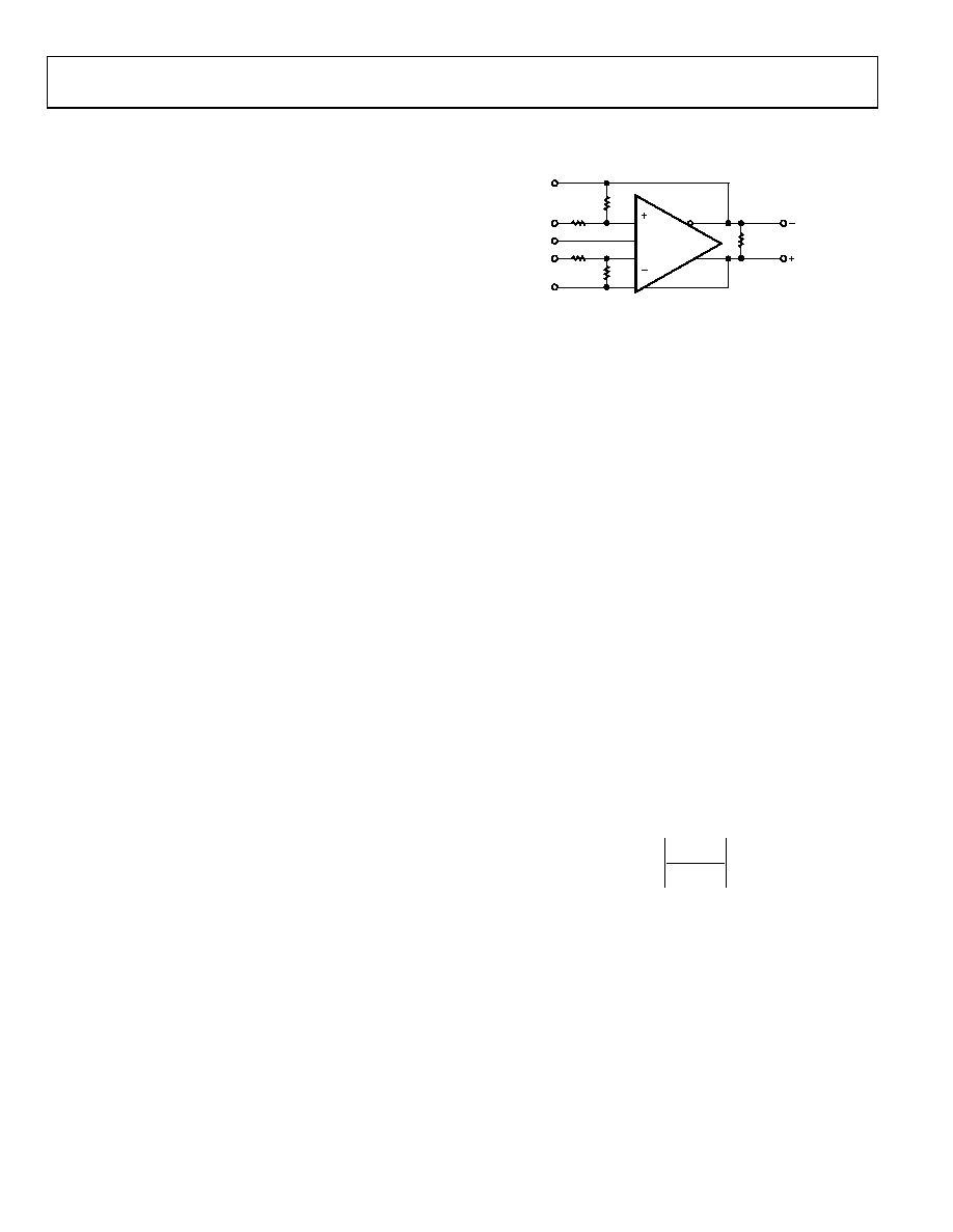
ADA4927
07
57
4-
0
46
Figure 46. Circuit Definitions
Differential Voltage
Differential voltage refers to the difference between two
node voltages. For example, the output differential voltage (or
equivalently, output differential-mode voltage) is defined as
VOUT, dm = (V+OUT VOUT)
where V+OUT and VOUT refer to the voltages at the +OUT and
OUT terminals with respect to a common ground reference.
Similarly, the differential input voltage is defined as
VIN, dm = (+DIN (DIN))
Common-Mode Voltage
Common-mode voltage refers to the average of two node voltages
with respect to the local ground reference. The output
common-mode voltage is defined as
VOUT, cm = (V+OUT + VOUT)/2
Balance
Output balance is a measure of how close the differential signals
are to being equal in amplitude and opposite in phase. Output
balance is most easily determined by placing a well-matched
resistor divider between the differential voltage nodes and
comparing the magnitude of the signal at the divider midpoint
with the magnitude of the differential signal (see Figure 44). By
this definition, output balance is the magnitude of the output
common-mode voltage divided by the magnitude of the output
differential mode voltage.
dm
OUT
cm
OUT
V
Error
Balance
Output
,
Δ
=
相关PDF资料 |
PDF描述 |
|---|---|
| ADA4930-1YCPZ-R2 | IC DIFF AMP 1.35GHZ 16-LFCSP |
| ADA4932-1YCPZ-RL | IC AMP DIFF LP 80MA 16LFCSP |
| ADA4939-2YCPZ-R7 | IC AMP DIFF DUAL ULDIST 24LFCSP |
| ADA4940-1ARZ-R7 | IC DIFF ADC DVR 18BIT LN 8SOIC |
| ADA4950-1YCPZ-RL | IC AMP DIFF LP 114MA 16LFCSP |
相关代理商/技术参数 |
参数描述 |
|---|---|
| ADA4927-2YCPZ-R7 | 功能描述:IC OPAMP CF DIFF DUAL LN 24LFCSP RoHS:是 类别:集成电路 (IC) >> Linear - Amplifiers - Instrumentation 系列:- 标准包装:2,500 系列:Excalibur™ 放大器类型:J-FET 电路数:1 输出类型:- 转换速率:45 V/µs 增益带宽积:10MHz -3db带宽:- 电流 - 输入偏压:20pA 电压 - 输入偏移:490µV 电流 - 电源:1.7mA 电流 - 输出 / 通道:48mA 电压 - 电源,单路/双路(±):4.5 V ~ 38 V,±2.25 V ~ 19 V 工作温度:-40°C ~ 85°C 安装类型:表面贴装 封装/外壳:8-SOIC(0.154",3.90mm 宽) 供应商设备封装:8-SOIC 包装:带卷 (TR) |
| ADA4927-2YCPZ-RL | 功能描述:IC OPAMP CF DIFF DUAL LN 24LFCSP RoHS:是 类别:集成电路 (IC) >> Linear - Amplifiers - Instrumentation 系列:- 标准包装:2,500 系列:Excalibur™ 放大器类型:J-FET 电路数:1 输出类型:- 转换速率:45 V/µs 增益带宽积:10MHz -3db带宽:- 电流 - 输入偏压:20pA 电压 - 输入偏移:490µV 电流 - 电源:1.7mA 电流 - 输出 / 通道:48mA 电压 - 电源,单路/双路(±):4.5 V ~ 38 V,±2.25 V ~ 19 V 工作温度:-40°C ~ 85°C 安装类型:表面贴装 封装/外壳:8-SOIC(0.154",3.90mm 宽) 供应商设备封装:8-SOIC 包装:带卷 (TR) |
| ADA4930-1 | 制造商:AD 制造商全称:Analog Devices 功能描述:Ultralow Noise Drivers for Low Voltage ADCs |
| ADA4930-1SCPZ-EPR2 | 制造商:Analog Devices 功能描述:ULTRALOW DIST LOW VLTG ADC DRIVER - Tape and Reel 制造商:Analog Devices 功能描述:Differential Amplifiers UltraLow Dist Low Vltg ADC Driver |
| ADA4930-1SCPZ-EPR7 | 制造商:Analog Devices 功能描述:ULTRALOW DIST LOW VLTG ADC DRIVER - Tape and Reel 制造商:Analog Devices 功能描述:IC OPAMP DIFF 1.35GHZ 16LFCSP |
发布紧急采购,3分钟左右您将得到回复。